PCBs for this project are available here.
Note: This tutorial will also work with the TDA2030 as long as you keep the supply voltage below ±18 V.
The TDA2050 is a great sounding chip amplifier with lots of power. In this tutorial, I’ll walk you through the amplifier design process as I build a 25 Watt stereo amplifier with the TDA2050. First, I’ll show you how to calculate the voltage and current requirements of your power supply, and show you how find a properly sized heat sink. Then, I’ll show you how to find the right values for all of the components in the circuit. I’ll also show you how to change the gain, and how to set the bandwidth of the amplifier. Finally, I’ll discuss PCB design and wiring the amplifier inside an enclosure. The information builds on itself, so it’s best to follow along in order. But if you want to jump ahead to a particular topic, here are links to the sections in this article:
- What to Know Before Starting
- Power Supply Voltage and Current
The datasheet is a good reference to have when building any amplifier. I recommend reading it before starting on this project:
WARNING!! THIS PROJECT INVOLVES HIGH VOLTAGES THAT CAN CAUSE SERIOUS INJURY OR DEATH. BE SURE TO USE PROPER SAFETY PRECAUTIONS, AND NEVER WORK ON A LIVE CIRCUIT.
You can also watch this video for an overview of the design process. At the end of the video I wire up the amp and play some music so you can hear what it sounds like:
What to Know Before Starting
Before you begin, you’ll want to get an idea of how much output power you want from the amplifier. You’ll also need to know the impedance of your speakers and the input voltage of your audio source. Be sure to check the TDA2050’s datasheet to find the absolute maximum ratings for these parameters, and design your amp to stay within the safe operating limits.
According to the datasheet, the TDA2050 can output 28 Watts into 4 Ω speakers with 0.5% distortion on a 22 V power supply. I’ll be powering 6 Ω speakers with my amplifier, so I’m going to aim for about 25 Watts output power. I’ll be using an iPhone as the audio source, which has a 1 V output voltage.
The first step is to figure out how much voltage and power you need from the power supply to get your desired output power.
Power Supply Voltage and Current
The TDA2050 can be powered from a split supply or single supply. The amplifier’s output power will be higher with a split supply, so that’s what I’ll use here.
Power Supply Voltage
Your desired output power and speaker impedance will determine how much voltage you need from the power supply. But before we can calculate the power supply voltage, we need to calculate the amplifier’s peak output voltage (Vopeak).
Peak Output Voltage
The peak output voltage can be found with this formula:
The peak output voltage of my 25 Watt amplifier driving 6 Ω speakers will be:
So with an output power of 25 Watts, the maximum voltage at the speakers will be 17.3 V.
Maximum Supply Voltage Needed by the Amplifier
Now you can find the maximum supply voltage (Vmax supply), which is the voltage your amp needs to get your desired output power. The supply voltage limit of the TDA2050 is ±25 V, so be sure not to exceed that.
The formula to calculate the maximum supply voltage is:
Regulation is the increase in transformer output voltage when there’s no load to draw current, which happens when the amplifier isn’t playing music. The exact value should be given in your transformer’s datasheet. The transformer I’ll be using has a regulation of 6%, so my maximum supply voltage is:
So, my power supply needs to deliver ±24.9 V for my amplifier to drive 6 Ω speakers at 25 Watts. The ± symbol means that the positive rail voltage is +25 V and the negative rail voltage is -25 V.
Maximum Supply Voltage Provided by a Transformer
The goal is to find a transformer that can output a maximum supply voltage close to the maximum supply voltage needed by your amplifier.
A transformer’s voltage rating only tells you its AC voltage output. The DC voltage you’ll get after the bridge rectifiers on the power supply convert AC to DC will actually be higher by a factor of 1.41. You’ll also need to account for surges in your mains supply, and the regulation of your transformer.
The maximum supply voltage you’ll get from a transformer can be calculated with this formula:
I started with a transformer rating of 15 V AC to see if that would provide the maximum supply voltage needed by my amplifier:
So a 15 V transformer will give me a maximum supply voltage of 24.7 V DC after the power supply. That’s really close to the 24.9 V maximum supply voltage needed for my amplifier, but now let’s calculate exactly how much output power I’ll get with it…
Amplifier Output Power from a Transformer’s Maximum Supply Voltage
This calculation is useful if you already have a transformer and want to see how much output power your amplifier will produce with it:
The maximum supply voltage from a 15 V transformer is 24.7 V, so the output power I’ll get from my amplifier is:
A 15 V transformer will give me 24.6 Watts of output power into 6 Ω speakers, and that’s close enough to my desired 25 Watts.
Transformer Power Needed by the Amplifier
Now we can determine how much power the transformer needs to supply the amplifier. Power is typically given as a VA rating in the transformer’s specifications. To calculate a minimum VA rating, we’ll first need to find the total power (Psupply) the transformer needs to supply the amplifier.
The total power depends on the maximum supply voltage you’ll get from the transformer, the amplifier’s peak output voltage, your speaker impedance, and the quiescent drain current (QDC) of the TDA2050 (90 mA):
So my 15 V transformer needs to supply at least:
Now we’ll use the total power to find a minimum VA rating for your transformer…
Convert Total Power to Transformer VA Rating
To find a minimum VA rating for your transformer, a general rule of thumb is to multiply the total power by a factor of 1.5.
For my 15 V transformer, the VA rating will need to be:
This is the VA per channel. For a stereo amplifier we just multiply by two:
So anything over a 150 VA transformer will supply my amplifier with enough power. This good to know because if your transformer is under powered, the amp might clip or distort the audio at higher volumes.
Finding the Right Heat Sink Size
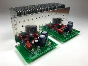
The two channels of my amplifier attached to a heat sink:
The TDA2050 needs to be attached to a heat sink or it will quickly overheat and get damaged. The size of the heat sink you need will depend on your maximum power dissipation and the thermal resistances in the path of heat flow away from the TDA2050.
Maximum Power Dissipation
The maximum power dissipation (Pdmax) is the amount of power the TDA2050 will dissipate as heat at the limit of it’s operation. Pdmax depends on the maximum supply voltage you’ll get with your transformer, and the impedance of your speakers:
According to the datasheet, the TDA2050’s absolute maximum rating for Pdmax is 25 Watts. If the Pdmax of your design is greater than 25 Watts, you’ll need to lower the supply voltage or increase the speaker impedance to prevent damage.
For the amplifier I’m building, the maximum supply voltage supplied by my transformer is ±24.7 V, and I’m driving 6 Ω speakers, so my Pdmax is:
A Pdmax of 20.6 Watts is below the TDA2050’s absolute maximum rating of 25 Watts, so everything looks good so far.
Maximum Thermal Resistance of the Heat Sink
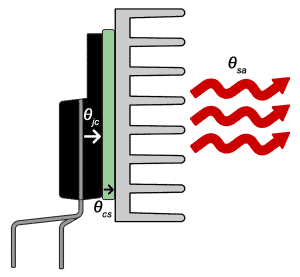
Now we can determine the maximum thermal resistance (in °C/W) of the heat sink you need to dissipate all of the power the TDA2050 produces. But before we can do that, we need to know the values of the three thermal resistances in the path of heat flow away from the TDA2050:
θjc: The thermal resistance from the chip’s junction (the die) to the exterior of the plastic case.
θcs: The thermal resistance from the chip’s case to the heat sink.
θsa: The thermal resistance from the heat sink to the ambient air.
Heat dissipation will be more efficient when any of these are made smaller. We can’t do anything to get a lower θjc, because it depends on the construction of the TDA2050’s package. θcs can be lowered by using thermal paste between the chip and the heat sink. The thermal resistance of thermal paste is usually around 0.2 °C/W, but check the datasheet to find the exact value for the type you’re using.
The largest reduction of thermal resistance will come from your choice of heat sink (θsa). Heat sink thermal resistance is usually provided as a °C/W rating in the datasheet or advertising material. Heat sinks with a lower thermal resistance will dissipate more heat.
Use this formula to calculate the heat sink’s maximum thermal resistance necessary to dissipate the TDA2050’s Pdmax:
- The θcs of the TDA2050 is 3 °C/W.
- Tjmax is the maximum junction temperature, or the temperature at which the thermal shutdown circuitry is enabled. Tjmax for the TDA2050 is 150 °C.
- Tamb is the ambient temperature (in °C) while the amplifier is operating. A typical value is room temperature (25 °C).
The maximum thermal resistance of the heat sink for my amplifier with a Pdmax of 20.6 Watts is:
So I’ll need a heat sink rated less than or equal to 2.9 °C/W to ensure it will dissipate all of the power my amplifier produces.
Calculating the Amplifier’s Component Values
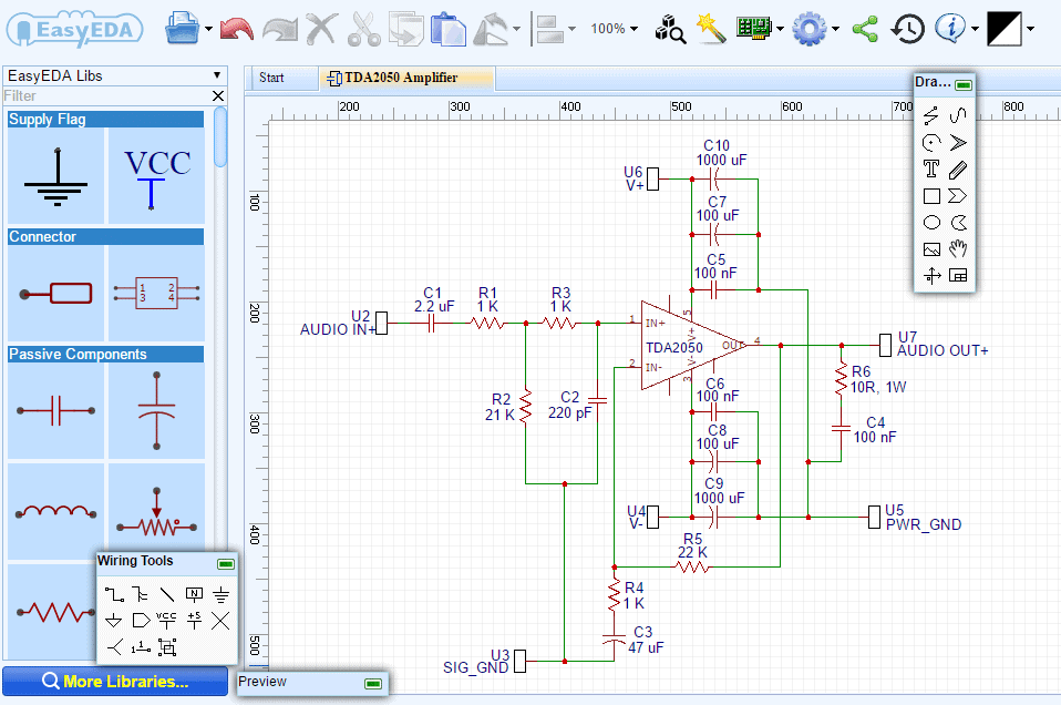
Now that all the power and heat sink requirements are figured out, let’s find the best values for the components in the circuit. I’ll use the schematic below, which is basically the same as the one in the datasheet, but with a few extra components to help filter noise:
If you click on the image you’ll be taken to the EasyEDA schematic editor where you can modify the circuit and change component values.
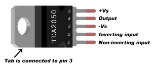
Here’s a diagram of the TDA2050’s pinout for your reference:
Minimum Gain
The gain of the TDA2050 should be set above 24 db to maintain stability, but there is also a minimum gain needed to get your desired output power. It depends on your input voltage, speaker impedance, and desired output power according to this formula:
I’ll be using an iPhone as the audio source for my amplifier. The iPhone has an output voltage of about 1 V, so to get 24.6 W output power, I’ll need to set the gain to at least:
This is expressed as the voltage gain (Vo/Vi), or the factor of amplification. To convert voltage gain to decibels gain, use this formula:
So setting my gain above 21.7 db will ensure that I get 24.6 Watts of output power. But the minimum gain of the TDA2050 is 24 db, so I’ll need to set it to at least 24 db.
Set the Gain
The values of resistors R4 and R5 set the gain of the TDA2050:
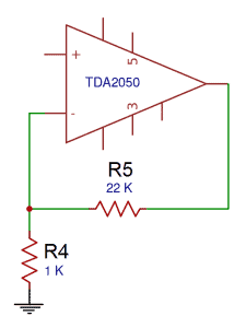
High gain settings will cause distortion and low gain settings may not provide enough volume. If your minimum gain value allows for it, a good gain to use for home listening is around 27 to 30 db. This setting isn’t high enough to cause distortion and will give you a good range of volume.
The best resistors for R4 and R5 are metal film types with tight tolerances. A tolerance of 0.1% or less is ideal. It’s important to use close tolerance resistors to set the gain, especially if you’re building a stereo amplifier. If the resistance values between the two channels are off by a few Ohms, the gains will be different and one side will be louder than the other.
The gain is calculated with this formula:
I’ll be setting the gain of my amplifier to around 27 db. I tried different resistor values with the formula above, and got close to my desired gain with R4 at 1 kΩ and R5 at 22 kΩ. These resistances will set my gain to:
Which will work fine since 27.2 db is above the minimum gain I calculated earlier, and above the 24 db minimum of the TDA2050.
Balance the Input Bias Current
After setting the gain, the next step is to balance your amplifier’s input bias current. The input bias current is the difference in currents flowing to the non-inverting input (pin 1) and the inverting input (pin 2). This difference in current needs to be minimized since it will create a DC voltage at the inputs that will be amplified as noise.
The current at inverting input is determined by the resistance of R5. The current at the non-inverting input is determined by the resistances of R2 and R3 in series:
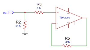
In order to make the currents at each input the same, we set
For my amplifier, I already found a value for R5 when I set the gain. For R3, I started with an arbitrary value of 1 kΩ then rearranged the formula above to find a value for R2:
So a 21 kΩ resistor for R2 and a 1 kΩ resistor for R3 will balance the input bias current.
Set the Low End of the Amplifier’s Bandwidth at the Input
Capacitor C1 prevents DC from the audio source getting to the amplifier’s input. If DC is allowed to reach the input, it will get amplified along with the audio signal and create noise.
C1 also forms a resistor-capacitor (RC) high pass filter with R2 that defines the low end of the amplifier’s bandwidth:
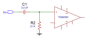
A filter’s cutoff frequency (Fc) is the frequency at which the filter starts to work. In a high pass filter, frequencies below the cutoff frequency are muted.
The cutoff frequency of this filter can be found with this equation:
We already found a value for R2 when we balanced the input bias currents. To find a value for C1, we just need to define a cutoff frequency. Since the lower limit of human hearing is 20 Hz, the Fc should be well below 20 Hz so that audible bass frequencies aren’t muted.
The Fc equation above can be rearranged to find the value for C1 at a particular cutoff frequency:
I went with an Fc of 3.5 Hz for my amplifier, but you can use slightly higher or lower values if you want. It may take some experimentation to find the perfect value for your ears, but just be sure to stay well below the lower limit of human hearing (20 Hz), or your amp’s bass response will be weak.
With an Fc of 3.5 Hz, the value of my C1 is:
C1 is directly in the input signal path, so it will affect your amplifier’s sound quality. For the best sound, use a polypropylene metal film or polypropylene metal film in oil capacitor.
Set the Low End of the Amplifier’s Bandwidth in the Feedback Loop
C3 and R4 form another high pass filter in the feedback loop:
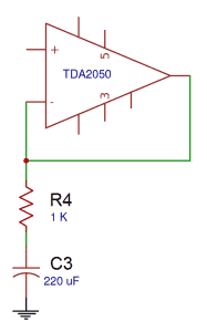
The cutoff frequency of this filter should be set 3 to 5 times lower than the cutoff frequency of the input high pass filter. If the cutoff frequency of this filter is higher than the filter at the input, low frequencies will be passed to the feedback loop filter that are below it’s cutoff frequency. This will create a DC voltage across C3 that will appear at the inverting input and get amplified as noise.
Even though the input filter sets the low end of the amplifier’s bandwidth, C3 still has an effect on the bass response. Smaller values of C3 will result in softer bass that has less punch, and larger values will make the bass tighter, with more impact.
Use the formula below as a starting point to find an ideal value for C3:
I already calculated values of R2, R3, R4, and C1, so my C3 should be greater than:
It’s going to be hard to find a 68 µF capacitor, so I’ll round up to 100 µF. Let’s see what the cutoff frequency would be with that:
Now lets check to see if 1.59 Hz is 3 to 5 times lower than the 3.5 Hz Fc of my input filter:
It’s 2.2 times lower, so maybe we can do better with a 220 µF capacitor. The Fc with a 220 µF capacitor is 0.72 Hz.
So a value of 220 µF for C3 sets the cutoff frequency of the feedback loop filter to 4.9 times lower than the cutoff frequency of the input filter. This will be just fine, so that’s what I’ll use.
Set the High End of the Amplifier’s Bandwidth
R1, R3, and C2 form a low pass RC filter at the amplifier’s input that defines the high end of the amplifier’s bandwidth:
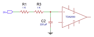
In a low pass filter, frequencies above the cutoff are muted. This filter has two functions. One, it sets the upper limit of the amplifiers’s bandwidth, and two, it filters high frequency radio and electromagnetic interference from the audio input.
The cutoff frequency of this filter should be greater than the 20 kHz upper limit of human hearing. It should also be lower than any radio broadcast frequencies that might be picked up by the input wires and traces.
The lowest radio broadcast frequency in the USA is AM at 535 kHz. I decided on a cutoff frequency of 350 kHz, which is well below 535 kHz and well above the 20 kHz upper limit of human hearing.
To find the value of C2 with an Fc of 350 kHz, I rearranged the cutoff frequency formula to solve for C2:
227 pF isn’t a common capacitor value. However, 220 pF would give an cutoff frequency of 362 kHz, so that will work fine as a substitute.
The Zobel Network
A Zobel network helps to prevent oscillation that can occur from the parasitic induction of speaker wires. It also acts as a filter to prevent radio interference picked up by the speaker wires from getting to the inverting input via the feedback loop.
C4 and R6 form a Zobel network at the amplifier’s output:
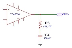
Since capacitors have a very low impedance at high frequencies, radio frequencies are shorted to ground via C4. R6 limits the high frequency current so there isn’t a direct short to ground, which could exceed the current limit of the TDA2050. The relatively low frequency audio current is blocked by C4, so it’s directed out to the speakers.
The cutoff frequency of the Zobel network can be calculated with:
The datasheet gives values for R6 = 10 Ω and C4 = 100 nF, which gives an Fc of:
159 kHz is above the 20 kHz limit of human hearing and well below radio frequencies, so these values will work fine.
If the amplifier oscillates, R6 will be passing high currents to ground so it should have a power rating of at least 1 Watt. C4 should ideally be a metal film capacitor with a low ESR, and a voltage rating greater than the rail to rail output swing.
Power Supply Decoupling Capacitors
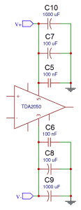
C5 to C10 are the power supply decoupling capacitors. They act as a reservoir of current that can be quickly supplied to the amplifier when needed. There is one set of decoupling capacitors for each voltage supply pin.
The larger value decoupling capacitors (C9 and C10) provide reserve current during extended periods of low frequency output. Larger values will improve the bass response of the amplifier.
The smaller value decoupling capacitors (C6 and C5) can supply reserve current rapidly for periods of intense high frequency output. They also filter high frequency noise and electromagnetic interference from the power supply.
Decoupling capacitors also compensate for the inductance and resistance of the power supply wires and traces leading to the chip. Inductance and resistance inhibit current flow, and since the main power supply is relatively far away from the TDA2050, the effect can be significant. Locating the decoupling capacitors as close as possible to the chip’s pins will maximize current flow to the chip.
The best types of capacitors to use will have a lower equivalent series resistance (ESR) and equivalent series inductance (ESL).
Grounding the Amplifier
Grounding is one of the most important aspects of amplifier design. A poor grounding layout can be a major source of hum and buzzing. A good grounding layout keeps the low current audio input and signal grounds separate from the high current power supply and speaker grounds. If high currents are allowed to flow through the low current grounds, a DC voltage will develop in the low current wires that will show up at the input and get amplified as hum.
To keep the different grounds separate, we’ll create several different ground networks:
- Audio input ground: For the ground wire of the audio input cable
- Signal ground: For the input circuit: R2, C2, and C3
- Speaker ground: For the speaker return wires
- Power ground: For the power supply decoupling capacitors and the Zobel network
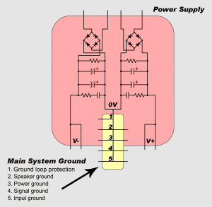
These grounds will connect to a group of terminals called the main system ground. The main system ground is connected to a ground loop protection circuit (I’ll explain more about this later), which then connects to the mains earth wire via the metal chassis.
The main system ground should be located as close as possible to the reservoir capacitors on the power supply:
The ground networks are connected to the main system ground in a particular order so that high currents only flow through the low current grounds for a very short distance. As shown in the diagram above, the ground loop protection circuit connection is closest to the reservoir capacitors and the input ground connection is the farthest away.
PCB Layout and Design
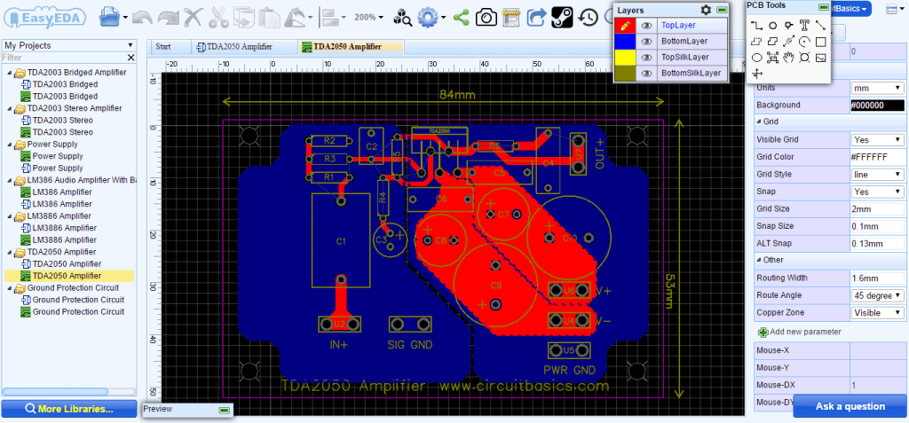
I designed the PCB for my amplifier using EasyEDA’s online PCB design software. EasyEDA is a full suite schematic and PCB design software/manufacturing service that’s free to use and offers great prices on custom PCB manufacturing. To edit the layout, change component footprints, and order the PCB, click on the image below:
The component labels on the PCB match the labels in the schematic
This PCB is for a single channel, so if you’re building a stereo amplifier you’ll need to build two boards. If you want some tips on designing PCBs and a tutorial on using EasyEDA, check out our article How to Make a Custom PCB.
PCB Ordering
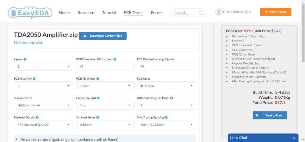
If you click on the “Fabrication Output” button in the PCB editor window, you’ll be taken to a page where you can order the PCB. You’ll also be given choices for copper thickness, PCB thickness, color, order quantity, and other parameters:
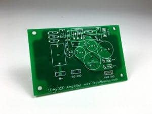
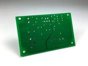
I ordered 5 PCBs and the cost came to $17.10 USD. Manufacturing and shipping took about 10 days. The boards came out great. The traces are routed precisely and all of the printing is very clear. Here’s one of the boards after manufacturing:
PCB Design Tips
There are four basic principles I took into account when designing this PCB:
- Current flowing through a conductor creates a magnetic field that can generate a current in a parallel conductor
- Current flowing in a conductive loop creates a magnetic field, and a magnetic field generates a current in a conductive loop. The magnitude of the current is proportional to the area inside the loop
- Inductance inhibits the flow of current. Long, thin traces have more inductance than short, thick traces
- A capacitor in series with an inductor creates a resonant circuit
The traces leading to the non-inverting input and feedback loop have been routed far away from the power supply and audio output traces to prevent high currents generating currents in low current traces. If routing a low current trace near a high current trace is unavoidable, run them at 90° angles, but never parallel. If you put the terminals for the high and low current circuits on opposite sides of the PCB, it will be easier to route them far away from each other.
Any space between traces of the same circuit will create a conductive loop that’s susceptible to receiving or transmitting magnetic fields. To avoid this, I’ve routed the positive and negative power supply traces close to each other, and used ground planes on the bottom of the PCB. When traces are routed over a ground plane, the width of the loop is reduced to the thickness of the PCB.
Since the power ground and signal ground need to be kept separate, the bottom side of the PCB has two ground planes that are not connected electrically. One ground plane carries the power ground, and the other ground plane carries the signal ground. On the top side of the PCB, the power supply traces, output, and Zobel network are routed over the power ground plane. The input and feedback loop traces are routed over the signal ground plane.
A capacitor in series with an inductor creates a resonant circuit, which can cause oscillation. Inductance also inhibits the flow of current. To reduce the effects of inductance, it’s best to keep all traces as short as possible. This is especially important for the power supply decoupling capacitors, the feedback loop, and the Zobel network. They’ve all been placed as close as possible to the chip’s pins to shorten the trace length.
Building the Amplifier
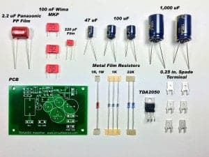
Assembling the PCB is pretty straight forward. Here are the components and PCB before soldering:
It’s usually easiest to solder the smaller components first, then work your way up to bigger components. I use a putty called Sticky-Tac to hold components in place on the top of the PCB while soldering from the bottom side.
If you can, use 63/37 eutectic solder instead of 60/40 tin lead solder. Eutectic solder has a smaller melting range which makes the solder bond set faster and gives a stronger bond. The melting range of 60/40 solder is fairly wide, and it become pasty at at the lower end of the range. If a component is moved in the pasty phase, the joint will be weak and may form a cold solder joint.
It’s also a good idea to use some fine grit sandpaper to remove any oxidation from the component leads before soldering.
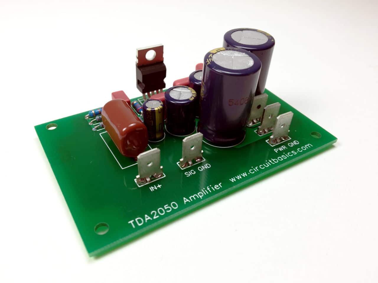
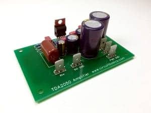
Here’s one channel of my amplifier after I soldered the components:
The Amplifier Enclosure/Chassis
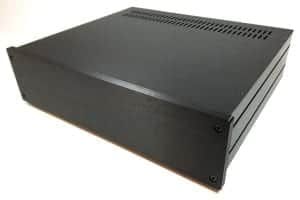
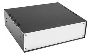
Metal enclosures are the most commonly used because they offer the best shielding from fluorescent light, radio frequency, and cell phone interference. It can be hard to find one that fits though. I recommend the enclosures from Hi-Fi 2000, a company in Italy that has beautiful enclosures available in lots of different sizes. The website is in Italian, but you can change the language to English. They also do custom printing, engraving, and drilling. I ordered their 330 mm X 280 mm Galaxy enclosure with a 10 mm black anodized aluminum front panel and it looks great:
But if you’re on a budget, their economy line looks really good too. The Economica 280 mm x 250 mm model would fit the stereo TDA2050 amplifier too:
Wiring the Amplifier
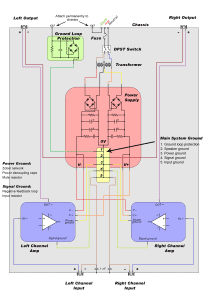
The diagram below shows how I wired my amplifier together inside the chassis:
Click on the image to view a larger version
To avoid interference from magnetic fields, try to keep the sensitive input and signal wires far away from the power supply wires, speaker output wires, transformer, AC mains wires, and rectifier diodes on the power supply.
To minimize the loop area, the following wires should be tightly twisted together for as long a distance as possible:
- AC hot and AC neutral wires to transformer
- 0 V and secondary voltage wires from transformer to power supply
- V+, V-, and power ground wires from power supply to amplifier PCB
- Speaker output and speaker ground
- Audio input and audio input ground
Three power supply wires (positive, negative, and power ground) run to each amplifier PCB. These wires should be thick and as short as possible to minimize the inductance. I used 14 AWG, but anything larger than 18 AWG should be fine.
The audio input and signal ground wires don’t carry a lot of current so they can be thin gauge. Solid core 22 AWG works really well and is easy to twist together.
For fault current protection, the mains earth wire should be secured to the chassis with a bolt, lock nut, and a ring terminal. Make sure to scrape off any paint or anodization from the chassis to get a good electrical connection. All metal parts (like the heat sinks) should also be electrically connected to the chassis.
The audio input ground and speaker grounds are wired directly from the terminals on the chassis to the main system ground.
Audio input cables from the source can pick up stray electromagnetic interference. To filter this out, you can install a 1 nF capacitor at each input terminal, from the positive side to ground.
The Ground Loop Protection Circuit
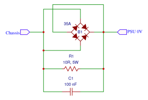
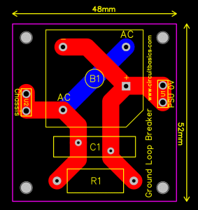
A ground loop is a current that flows from the audio source to the amplifier through the ground shield of the audio input cables. This current will be picked up at the amplifier’s input and produce an annoying hum. You can use an extra circuit placed between the main system ground and the chassis connection to break the ground loop current:
NOTE: THIS CIRCUIT MAY NOT BE LEGAL IN YOUR AREA. PLEASE CHECK YOUR LOCAL ELECTRICAL CODES OR CONSULT AN ELECTRICIAN BEFORE USING A GROUND LOOP BREAKER
Under normal operating conditions, low voltage ground loop currents flow through the resistor (R1). The resistor reduces this current and breaks the ground loop. If a high current fault occurs, the fault current can flow through the diode bridge to earth. The capacitor filters any radio frequencies picked up by the chassis.
The main system ground connects to the ground loop protection circuit at the “PSU 0V” terminal. The ground loop protection circuit then connects to the chassis from the “Chassis” terminal. The connection to the chassis can be at the same bolt where the mains earth wire connects, or at another spot.
If you use a ground loop protection circuit, be sure to isolate all input and output connectors from the chassis. Otherwise, there will be a direct path from the main system ground to the chassis and the ground loop protection circuit will be bypassed entirely.
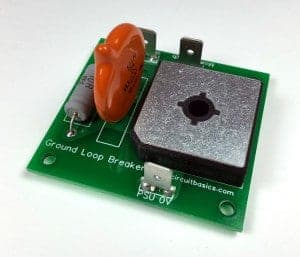
The ground loop protection circuit can be hard wired, but it’s a little neater to mount the components to a PCB:
Click on the image to edit the layout, change component footprints, and order PCBs.
How Does it Sound?
Overall, the amp sounds great. The bass, mids, and treble are all very clear and well balanced. It also has plenty of power. There’s more than enough volume for listening in my living room. There is no hum or noise while the amp is powered on and plugged into the source.
While the sound quality of the TDA2050 may not be up to par with our Hi-Fi LM3886 amplifier project, it still sounds really good. If this is your first amplifier build, I’d suggest starting with our TDA2003 stereo or bridged amplifier projects since they’re quite a bit easier to build.
Be sure to leave a comment if you have any questions, and feel free to share this post if you know anyone that would find it useful! Thanks for reading…






how we find voltage drop across TDA2050
Hi! I loved this tutorial, it is very handy and detailed, but I have a small problem which would be nice if someone could answer.
How did you get the voltage drop of the IC (4V) at the equation? I cannot figure it out. I thought that it is the minimum operating voltage of the ic maybe, but it is actually 4.5V. Thank you in advance for the response. Have a nice day ;)
Sorry, I wanted to post this as a comment, not a reply, I will corect my mistake. :)
Thank you so much for this article and the website. It’s the first tutorial I’ve read that shows me all the basic calculations required to design an amplifier. It is so coherently written and is so complete. Providing all the equations helped me enormously. I feel I may have a chance at building an amp now.
PS: The diagram immediately under “Amplifier Output Power from a Transformer’s Maximum Supply Voltage” has an extra “(10” showing. I don’t speak Latex very well, so I can’t tell what the command should be.
Glad you found it helpful! Thanks for noticing the Latex error… That’s supposed to be “(10%)”. Just fixed it.
Can I know the voltages of the capacitors?
What you used?
I think the rule of thumb is to use 2x the maximum voltage passing through that particular cap.
So if the power supply voltage is 18v, use at least a 36v cap in the P.S. circuit. More likely 50v, as this is a common value.
That’s my understanding at least. I’m here to learn too.
I want to Thank You so much for this article.
Best description and analysis
please can somebody help,
i dont know how to calculat decoupling capacitor
because i see the circuit valu of decoupling capacitor
i need to explain me
thnx
big up! will you provide the circuit diagram soon?
Hello, how can i add a volume pot in the circuit?
And also, wich are the Power Supply components value?
thanks you!!
HI, this is an excellent article, thank you very much. I am just slightly confused about the transformer specification though. I can follow all of your reasoning as it’s very clear and well presented, which results in a dual 15V 150VA toroidal transformer, however on the parts list the transformer seems to be listed as a dual 18V 300VA? Is this a copy and paste error from another project that requires a higher voltage and VA rating? Or am I missing something?
thanks for article helped me a lot with my project
wow DIY will help to save amplifier cost.. i tried it your guide and its working great..
thanks for this awesome guide
Thank you so much for the article.
Can you please publish an amplifier build using the TDA7294 IC?
nice bro
Nice one
good works, good days!
if we can make a tda2050 bridge circuit that we can work with single feed, can you send such a scheme
SIR, C3 which sets the low end of the amplifier bandwidth is required to be above 68 MIC as per your calculation.
Yet in the EDA diagram and parts list is given as 48 MF.Your recommended value is 220MF.
Is this an inadvertent error ? Could you please explain?
Thanks
Correction 68MF not 68 MIC, TYPO
YES! I had the same question! I also noticed the discrepancy between the value that he said he would use in the final calculation paragraph of 220uF, but later on down the page in the EDA diagram and in the parts list, it ends up being a 47uF instead apparently, with no explanation of why it changed… But the 47uF shown and used on the final circuit board isn’t even as high as his very first initial calculation of what would work as a minimum of 68uF, so I don’t understand what happened there either…
Hopefully the writer/publisher of this otherwise very detailed and good article will read and reply to all of these comments that people have about this circuit, especially the more critical design aspects of it like this! Let’s keep our fingers crossed that they will reply soon, because I’d very much like to try this circuit design out for myself to see how it will sound!…
Although it’s really too bad that the original TDA2050 chip isn’t being produced anymore by ST, so now all that you can find to buy online are fake, lesser quality copies of it by other China manufacturers, which don’t even come close to the same performance level (or safety level) of the original ST made chips! Maybe I can get lucky and find someone who still has some of the original, “new, old stock” chips from ST available to buy…
I have a few questions about this design:
First off, your Parts List link towards the top of the page doesn’t work. When you click on that link all it does is take you to the exact same page that you’re already on, i.e. the entire “how to build…” page itself. It would be nice if you could fix that so we can see all of the values for everything, including especially all of the power supply components; the bridges’ current capacities and voltage ratings, all of the main filter capacitor values, voltages, and types, etc, etc.! (Of which you mention nothing detailed about the power supply design in the article, even though the power supply is one of THE MOST IMPORTANT aspects of any great amplifier!!)
Please also show what kind of Volume control circuit can be best used for the input of this! I would like to build a portable mini amplifier from this project that I would be able to take out into the field with me and use it to test speakers, source components and other audio things when I find them used at thrift stores, garage sales, etc., so having its own volume control on it would be extremely helpful and essentially necessary!
What in the world is such a ridiculously huge bridge rectifier for in the ground loop isolation circuit??! Why not just use a diode, or back to back polarity diodes for that part of the circuit instead of that crazy big bridge? I understand why ground isolation is important, but why is that specific bridge rectifier necessary, (and why is it so huge), anyway? (It seems like that part of the circuit is “major overkill” and just a waste.)… Please explain further.
Why the Capacitor value discrepancy on C3 from the design paragraph 220uF “value that I will use”, to the ending result on the actual circuit board of only 47uF? What happened there and why?
Thanks!
Never thought that making an amplifier with the TDA2050 is so easy. I will be making this for my project and the details are enough for writing the theoretical aspects in my lab notebook.
Wow, this is awesome, thanks for posting this, I just have one question: what if I want to change the volume of the amplifier? I mean, I know I just have to add a variable resistor, but would it be too much trouble?
A repeat from Lm3886 block
Hi, i am confuse this is what we can read in your Guides,
for LM3886
“Audio input cables running from the source to the amplifier chassis can pick up interference. If this becomes a problem, you can install a 1 nF capacitor between each input terminal ground and the chassis to filter it”.
For TDA 2050:
“Audio input cables from the source can pick up stray electromagnetic interference. To filter this out, you can install a 1 nF capacitor at each input terminal, from the positive side to ground”.
which one is right?? from the positive to ground or from ground to chassis
Oh than ks and nice info from thre.
Dear sir we have to apply dc volatge ppwer from bridge rectifieri to the Vs pin along with three decoupling cpacitor or ac??
Hi! I loved this tutorial, it is very handy and detailed, but I have a small problem which would be nice if someone could answer.
How did you get the voltage drop of the IC (4V) at the equation? I cannot figure it out. I thought that it is the minimum operating voltage of the ic maybe, but it is actually 4.5V. Thank you in advance for the response. Have a nice day ;)
Oh than ks and nice info from thre.
i have difficult time
try to calculate power and voltage
for
tweeter 4 ohm (30 watt max) SB19ST-C000-4
woofer 8 ohm (40 watt max) SB16PFC25-8
this is speakers specs
http://www.sbacoustics.com/index.php/products/tweeters/dome/sb19st-c000-4/
http://www.sbacoustics.com/index.php/products/midwoofers/pfc/6-sb16pfc25-8/
Tuan …saya adalah pemula … dan telah bisa membuat amplifier tda 2050 untuk kamar saya … walau tidak sama persis dengan yang penulis berikan … dan sekarang saya mau belajar membuat amplifier dengan IC tda7284 … bisakah saudara penulis menjelaskan skema dan circuit tda 7294 kepada saya …. Terima Kasih .
This is the best comprehensive tutorial I’ve seen on building an amp from scratch., or any subject for that matter.
I appreciate anybody putting effort into teaching any subject, but sometimes I leave more frustrated than when I arrived.
Not here. No assumption that we should just understand something without a thorough explanation.
I have never taken a course in electronics, so I need the rudimentary lessons AND the more complicated formulas.
Very much appreciated. You’re doing Yeoman’s work here.
Thanks.