Note: Editable PCB files are available for this project here.
The LM3886 is one of the most highly regarded audio chip amplifiers in the DIY community. The reason for its popularity is due to its very low distortion, minimal external components, and low cost. With the right layout and component selection, you can build an excellent sounding Hi-Fi audio amplifier that will rival high-end amps retailing for several thousand dollars or more.
In this tutorial, I’ll go step by step through the amplifier design process as I build a 40 Watt stereo amplifier using the LM3886. I’ll explain what each part of the circuit does, and show you how to calculate the right component values with examples from the amplifier I’m building. I’ll also show you how to layout the PCB and wire the amplifier in an enclosure for minimal noise and hum.
My amplifier is based off of the same circuit provided in the datasheet, with all of the optional stability components included.
I highly recommend reading the datasheet before building your amplifier. It has all of the performance specifications, absolute maximum ratings, schematics, and design tips:
Application note AN-1192 has additional information that fills in gaps left out of the datasheet. It also has schematics for bridged and parallel amplifier circuits:
![]() Overture Application Note AN-1192
Overture Application Note AN-1192
It’s also good to have the Overture Design Guide. This is an Excel spreadsheet that calculates output power, heat sink size, gain, and other useful parameters:
Since this is a rather long article, here are links to the different sections:
- Things to Decide Before Starting
- Determine the Required Power Supply Voltage and Power
-
- Required Power Supply Voltage
- Required Transformer Power
- Determine the Proper Heat Sink Size
- Calculating the Component Values
- Find the Minimum Gain Required
- Setting the Gain
- Balancing the Input Bias Current
- Set the Low Frequency Cutoff at the Amplifier’s Input
- Set the Low Frequency Cutoff at the Feedback Loop
- Set the High Frequency Cutoff at the Amplifier’s Input
- Stability Components Rf2 and Cf
- The Zobel Network
- The Thiele Network
- Power Supply Decoupling Capacitors
- The Mute Circuit
- The Final Schematic
- Designing the Ground Layout
- Designing the PCB Layout
- Wiring it All Together
- How Does it Sound?
-
You can also check out this video to see a quick overview of the design process. At the end I wire up the amp so you can hear what it sounds like:
Things to Decide Before Starting
Before starting to design your amplifier, you should have an idea about how much output power you want to get out of it. Output power is what you’ll typically see stated as the Wattage rating of an amplifier. The maximum output power of the LM3886 is 68 Watts, but the actual power you get will depend on your power supply voltage and speaker impedance.
You’ll also need to know the impedance of your speakers. You should be able to find your speaker’s impedance on the back of the speaker or in the user manual.
Finally, you’ll need to know your input voltage. This is the output voltage of the audio source you’ll be amplifying. It may be in the device’s user manual, but if not, you can get a rough estimate by playing a 60 Hz pure sine wave (there are apps that will do this) at full volume and measuring the AC voltage between ground and the left or right channel with a multi-meter.
WARNING: THIS PROJECT INVOLVES WORKING WITH MAINS SUPPLY VOLTAGES THAT CAN SERIOUSLY INJURE YOU OR KILL YOU. BE SURE TO TAKE ALL NECESSARY SAFETY PRECAUTIONS, AND NEVER WORK ON A LIVE CIRCUIT!!
Determine the Required Power Supply Voltage and Power
Let’s start by figuring out how much voltage and power your amplifier will need from the power supply. These calculations will tell you the correct voltage and VA ratings for the transformer you’ll use to power your amp. This step is important because if the transformer’s voltage is too low, the output power of the amplifier will be less than what you expected. If the transformer’s VA rating is too small, the amplifier might clip or distort the audio at higher volumes.
Required Power Supply Voltage
Before you can find the required power supply voltage, you need to calculate the amplifier’s peak output voltage.
Find the Peak Output Voltage
Peak output voltage (Vopeak) is the maximum voltage measured across the amplifier’s speaker terminals. Your amplifier’s peak output voltage will depend on your desired output power (Po) and speaker impedance, according to this formula:
The amplifier I’m building will be 40 Watts with 6 Ω speakers, so my peak output voltage is:
Find the Maximum Supply Voltage Needed by the Amplifier
Now that you’ve found the peak output voltage of your amplifier, you can calculate the maximum supply voltage (Vmax supply). This is the voltage the amplifier needs from the power supply to get the desired output power.
To find the maximum supply voltage, take the peak output voltage and add the voltage drop (Vod) of the LM3886 (4 V). Then factor in your transformer’s regulation and the variation in your mains voltage.
Regulation is the increase in output voltage of a transformer when the load isn’t drawing current (i.e. the amp stops playing music). Regulation values can usually be found in the transformer’s datasheet, but if you don’t know your transformer’s regulation, a safe value to use is 15%. The regulation of the transformer I’ll be using is 6%.
Mains voltages can vary up to 10% depending on your location. It usually peaks late at night when people are asleep and drops in the daytime when more people are awake and drawing current from the power grid.
Use this formula to calculate the maximum supply voltage required by your amplifier:
For my 40 Watt amplifier, the maximum supply voltage it needs is:
So my power supply will need to deliver a peak voltage of ±30.2 V for my amplifier to output 40 Watts into 6 Ω speakers. The ± symbol indicates that the voltage is +30.2 V on the positive rail and -30.2 V on the negative rail.
The next step is finding a transformer voltage rating that can deliver this maximum supply voltage.
Find the Maximum Supply Voltage Output by a Transformer
Keep in mind that a transformer’s voltage rating only tells you it’s AC voltage output. The DC voltage will be higher after the bridge rectifier diodes on your power supply convert the AC voltage to DC.
To find the maximum DC supply voltage output by a transformer and power supply, take the transformer’s AC voltage rating and factor in a 1.41 increase in voltage from the rectifier diodes, the 10% mains supply variation, and the transformer’s regulation:
I tried the above calculation with a transformer rated at 18 V AC to see if it could supply the 30.2 V maximum supply voltage needed by my amplifier. With an 18 V transformer, I would get a maximum supply voltage of:
29.6 V is pretty close to the 30.2 V maximum supply voltage needed by my amplifier, but let’s calculate exactly how much output power I’d get with this transformer.
Find the Output Power from a Transformer’s Voltage Rating
To calculate the output power you’ll get from a particular transformer’s voltage rating, use this formula:
Using the maximum supply voltage I calculated for an 18 V transformer (29.6 V), the output power I’ll get is:
38.2 Watts of output power is pretty close to my goal of 40 Watts, so an 18 V transformer will work fine.
Required Transformer Power
Now let’s find a minimum VA rating for the transformer that will power your amplifier.
First you’ll need to calculate the total power (Psupply) required by the amplifier. Total power depends on the maximum supply voltage output by the power supply, the amplifier’s peak output voltage, and the speaker impedance. The formula to use is:
I’ve already calculated the maximum supply voltage of an 18 V transformer (29.6 V), and the peak output voltage of my amplifier (21.9 V). The total quiescent power supply current (QPSC) is given in the LM3886’s datasheet as 85 mA.
So my 18 V transformer needs to supply the amplifier with at least:
The total power can now be used to find a minimum VA rating for your transformer.
Convert the Total Power to a Transformer VA Rating
To convert the total power to a transformer VA rating, a general rule of thumb is to multiply it by a factor of 1.5:
This is the VA required for each channel, so for a stereo amplifier powered by a single transformer, just double it:
Finding a transformer with a VA of 222 will be hard, but you can round-up to the next closest value and use a 250 VA transformer or larger.
Determine the Proper Heat Sink Size
The LM3886 needs a heat sink large enough to dissipate the heat it generates or it will quickly become damaged. The minimum size of the heat sink can be found by calculating its maximum thermal resistance (in °C/W).
First though, you’ll need to know your LM3886’s maximum power dissipation (Pdmax), and the thermal resistances in the path heat takes from the chip die to the ambient air.
Find the Maximum Power Dissipation
The maximum power dissipation is the limit at which the LM3886’s internal SPiKe circuitry is enabled. Sound quality is severely compromised when the SPiKe circuitry is enabled, so to prevent this we need a heat sink with a thermal resistance low enough to dissipate the maximum power dissipated by the LM3886. Pdmax depends on the maximum supply voltage of your power supply and your speaker impedance:
The maximum supply voltage output from my power supply is ±29.6 V, and I’ll be driving 6 Ω speakers, so my Pdmax is:
So my heat sink needs to be able to dissipate 29.6 Watts of power to prevent activation of the SPiKe protection circuit.
Find the Maximum Thermal Resistance of the Heat Sink
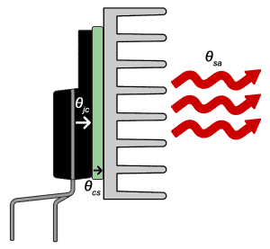
There are three resistances to heat flow away from the LM3886:
θjc: The thermal resistance from the chip’s junction (the die) to the case.
θcs: The thermal resistance of the gap between the chip case and the heat sink.
θsa: The thermal resistance from the heat sink to the ambient air.
More power will be dissipated when any of the thermal resistances in the path to ambient air are lowered. θjc is a property of the plastic case enclosing the die, so we can’t do anything to lower that.
θcs can be lowered by using a thermal paste between the chip and the heat sink. Thermal paste has a thermal resistance of around 0.2 °C/W, but the exact value of the type you use should be available from the manufacturer.
The most effective way to reduce the total thermal resistance is by lowering θsa with a more efficient heat sink. Heat sinks with a lower θsa are better at dissipating heat.
The heat sink will dissipate the peak power produced by the amplifier (Pdmax) if its thermal resistance (θsa) is less than or equal to the value calculated with this formula:
The LM3886 is manufactured in two different packages, the LM3886T and the LM3886TF. The LM3886T has a metal flange on the back of the case, and the LM3886TF is all plastic. The plastic case of the LM3886TF gives it a higher θcs:
- LM3886T: θcs = 1 °C/W
- LM3886TF: θcs = 2 °C/W
Tjmax is the maximum junction temperature, or the temperature at the chip’s die above which the thermal shutdown circuitry is enabled. The datasheet gives a value for Tjmax of 150 °C.
Tamb is the ambient temperature in °C that the amplifier will be operated at. A typical value for Tamb is room temperature (25 °C).
So the maximum thermal resistance (θsa) of the heat sink for my amplifier with a Pdmax of 29.6 W is:
So I’ll need a heat sink rated at less than or equal to 2.1 °C/W to ensure it can dissipate the maximum power produced by the LM3886.
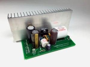
Here’s one channel of my amplifier attached to a properly sized heat sink:
Calculating the Component Values
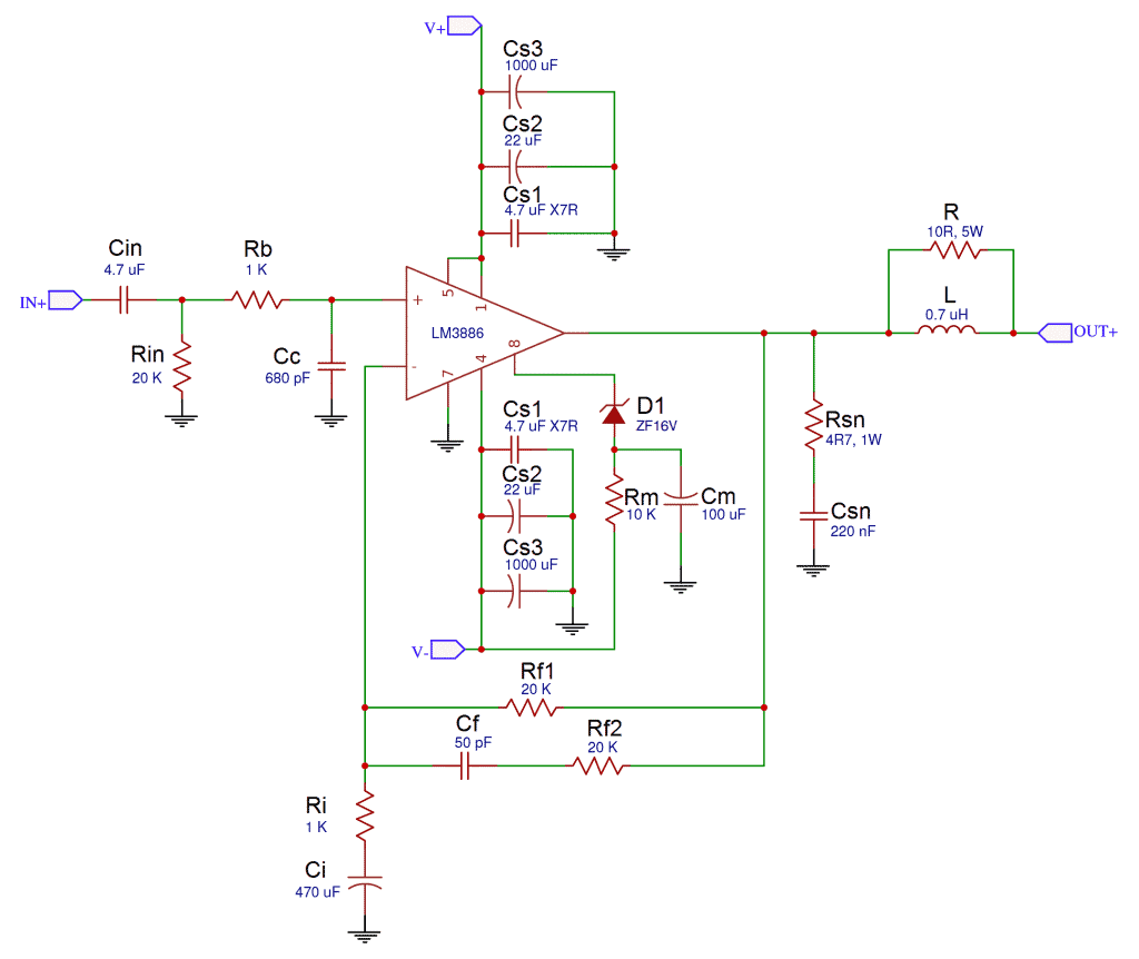
Now that you’ve calculated the power supply and heat sink requirements, the next step is to find values for the components in the amplifier circuit. I’ll be using the schematic below. It’s basically the same as the one in the datasheet, but with the optional stability components included:
Note: The components are labeled as they appear in the datasheet.
Here’s a diagram of the LM3886’s pin layout for your reference:
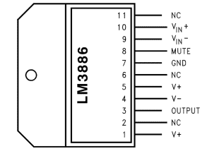
Find the Minimum Gain Required
The gain can be set to any value above the LM3886’s minimum of 10 Vo/Vi, but in order to get your desired output power, it needs to be above a certain minimum value. The minimum gain setting of your amplifier will depend on your input voltage, speaker impedance, and output power according to the formula:
I plan on using an iPhone as the audio source for my amplifier, which has an output voltage of 1 V. The output power I’ll get with my transformer and power supply is 38.2 W, and the impedance of my speakers is 6 Ω. So my minimum gain is:
So I’ll need to set the gain to at least 15.1 Vo/Vi if I want 38.2 Watts output power into 6 Ω speakers with a 1 V input voltage.
Setting the Gain
The gain of the LM3886 can be set by changing the values of resistors Ri and Rf1. These resistors form a voltage divider that determines the voltage at the inverting input (pin 9) of the LM3886:
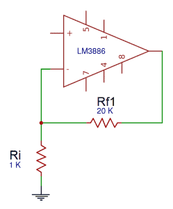
Setting the gain too high might cause distortion. Setting it too low might make your amplifier too quiet. A good gain setting that’s not too high to cause distortion, but not too low to give you a good range of volume is around 27 to 30 db.
The gain is calculated with this formula:
This gives you the voltage gain (Vo/Vi), or the factor of amplification. To convert voltage gain to decibels (db) gain, use this formula:
Higher value resistors create more Johnson-Nyquist noise, so it’s best to find an Rf1 / Ri ratio that provides your target gain with low resistor values.
I decided on a gain of around 27 db (22.4 Vo/Vi) for my amplifier. To keep the resistances low, I started out by setting Ri to 1 kΩ. Then I rearranged the gain formula to solve for Rf1 with a gain of 22.4 Vo/Vi:
I’m going to use Vishay-Dale PTF series metal film resistors throughout my amplifier, but the closest value I could find was 20 kΩ. But using a 20 kΩ resistor for Rf1 would make the gain:
Which is close enough to 27 db, and above the 15.1 Vo/Vi minimum gain required for my desired output power, input voltage, and speaker impedance.
If you’re building a stereo amplifier, you want Ri and Rf1 to have close resistance tolerances. If these resistors vary much between the two channels, the gains will be different and one channel will be louder than the other. Metal film resistors with a tolerance of 0.1% or less are ideal.
Balancing the Input Bias Current
After setting the gain, the next step is to balance the input bias currents by choosing values for Rin and Rb:
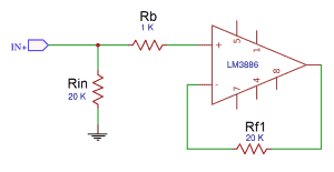
If the currents at the non-inverting input (pin 9) and the inverting input (pin 10) are different, a voltage will develop between them. This difference in voltage will be amplified as noise.
The inverting input sees the resistance of Rf1 and the non-inverting input sees the resistance of Rin and Rb in series. You already found a value for Rf1 when you set the gain of the amplifier. The values of Rin and Rb are chosen so together they equal the value of Rf1. This will make the current at the non-inverting input equal to the current at the inverting input. To find values of Rin and Rb for a particular Rf1, use this formula:
I used the value given in the datasheet for Rb (1 kΩ). So with Rf1 at 20 kΩ, the value of Rin that balances the input bias current for my amplifier is:
You’ll probably be able to find a 19 kΩ resistor available with the type of resistors you’re using, but 20 kΩ is the closest value I could find with Vishay-Dale PTF resistors so I’ll have to settle with that.
Set the Low Frequency Cutoff at the Amplifier’s Input
Cin is in series with the non-inverting input. It’s main function is to block any DC present in the audio source, while allowing AC (the audio signal) to pass. DC in the audio source needs to be blocked or it will be amplified along with the audio signal and create a high DC offset at the speakers. This distorts the audio, which we don’t want for obvious reasons.
In addition to the DC blocking function, Cin and the input resistor (Rin) form a high pass RC filter that sets the low end of the amplifier’s bandwidth at the non-inverting input:
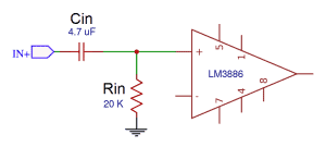
This filter’s cutoff frequency (also known as the -3db point or corner frequency) is the frequency at which the filter starts to work. In a high pass filter, frequencies below the cutoff frequency will be attenuated (muted). In a low pass filter, all frequencies above the cutoff frequency will be muted. We’ll use combinations of low pass and high pass filters to set the amplifier’s bandwidth and improve stability.
The cutoff frequency (Fc) of this filter can be found with the equation:
The equation can be rearranged to find a value of Cin for a particular Fc:
You found the value for Rin when you balanced the input bias currents, so all you need now is to choose a cutoff frequency. The lower limit of human hearing is 20 Hz, so the Fc should be well below that to prevent attenuation of bass frequencies. Lower than 2 to 4 Hz is ideal.
I tend to listen to music with lots of bass, so I decided on a fairly low Fc for my amplifier. I started with 1.5 Hz, but you can use higher or lower values if you want. Just be sure to stay well below 20 Hz or the bass will be weak.
With an Fc of 1.5 Hz, the value of my Cin needs to be:
A 5.3 µF capacitor will be hard to find, but a close value that’s fairly common is 4.7 µF. The Fc with a 4.7 µF capacitor would be:
An Fc of 1.69 Hz is pretty close to my desired 1.5 Hz, so a 4.7 µF capacitor should be good.
Since Cin is directly in the path of the audio input signal, the type of capacitor used will have an influence on sound quality. Electrolytics, ceramics, and tantalum capacitors should be avoided. A good quality polypropylene metal film, or even better a polypropylene metal film in oil capacitor will sound best here.
Set the Low Frequency Cutoff at the Feedback Loop
A second high pass filter exists in the feedback loop with Ri and Ci:
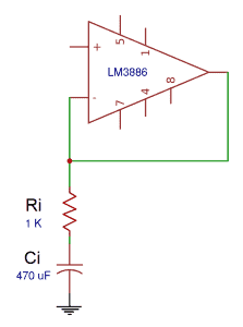
The cutoff frequency of this filter should be 3 to 5 times lower than the Fc of the Cin\ Rin high pass filter at the input. If the Fc of this filter is higher than the input filter, the amplifier will pass low frequencies to the feedback loop that it can’t handle. This will create a voltage across Ci and cause DC voltage to appear at the inverting input, which will be amplified and cause distortion. Therefore, the input filter (Cin and Rin) should determine the lower bandwidth frequency of the amplifier, not the feedback loop filter (Ci and Ri).
The input filter defines the low end of the bandwidth, but Ci still has an effect on the bass response. With smaller values of Ci, the bass will be softer and have less punch, but with larger values of Ci, the bass will be tighter and have more impact.
The formula below will give you a starting point for the value of Ci:
I already found values for Rin, Cin, Rb, and Ri, so the value of my Ci should be greater than:
Rounding up to the next common capacitance value gives 220 µF. Lets see what the cutoff frequency would be with that. We can use the Fc equation with Ri and Ci:
Now I’ll check to see if 0.72 Hz is 3 to 5 times lower than the 1.69 Hz Fc of my input filter:
It’s 2.3 times lower. Lets try some larger values for Ci to see if we can’t do better than that. Repeating the Fc calculation for a 330 µF capacitor gives 0.48 Hz.
3.5 times lower is okay, but I might be able to do even better with a 470 µF capacitor. Repeating the calculations again with a 470 µF capacitor gives an Fc of 0.34 Hz.
A 470 µF capacitor will set the Fc of my feedback loop filter to 4.9 times lower than the Fc of my input filter. This is great, so I’ll use a 470 µF capacitor for Ci.
Ci is also in the audio signal path, so a good quality capacitor should be used. The capacitance will probably be too high to use polypropylene, so you’ll likely have to use an electrolytic. However, there are good quality audio grade electrolytics like the Elna Silmic II or Nichicon KZ series which shouldn’t adversely affect the sound quality.
Set the High Frequency Cutoff at the Amplifier’s Input
Rb and Cc form a low pass RC filter that sets the upper limit of the amplifier’s bandwidth at the non-inverting input:
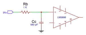
In the datasheet, Cc is shown connected between the non-inverting input and the inverting input. In that configuration, Cc filters radio frequency and electromagnetic interference picked up by the input wires. Unfortunately, it also increases the chance for oscillation. A better way is to connect Cc from the non-inverting input to ground as shown in the image above. That way Cc still filters radio frequencies, but it also acts as a low pass filter that will set the upper limit of the amplifier’s bandwidth.
The Fc of this filter should be set well below the lowest radio broadcast frequency in your area, and well above the 20 kHz upper limit of human hearing. Broadcast radio frequencies in the USA are:
- FM: 87.5 to 108 MHz
- AM: 535 to 1605 kHz
I chose to start with an Fc of about 250 kHz. It’s well below the lowest AM broadcast frequency (535 kHz), so radio frequencies and most electromagnetic interference should be filtered out. It’s also well above the upper 20 kHz frequency of human hearing, so higher audio frequencies won’t be attenuated.
To find a value for Cc that gives an Fc of 250 kHz, I’ll just rearrange the cutoff frequency formula:
Since 636 pF is not a common value, I’ll round up to 680 pF. With a 680 pF capacitor, the Fc becomes:
So a 680 pF capacitor will set the upper cutoff frequency to 234 kHz, which is close enough to my desired Fc of 250 kHz. Cc is also in the signal path, so a good quality capacitor should be used. The best dielectric types for audio capacitors in the picofarad range are silver mica or polystyrene.
Stability Components Rf2 and Cf
Rf2 and Cf dampen resonance in the feedback loop and enhance stability:
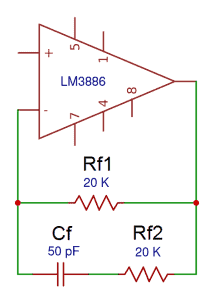
Rf1, Rf2, and Cf form a low pass filter in the feedback loop, but as you can see from the formula in the datasheet, calculating the Fc of this filter is quite complicated:
The best way to determine values for Rf2 and Cf is with circuit simulation software such as LTSpice. That’s beyond the scope of this article though, so I’m just going to use the values given in the datasheet.
But if you want to experiment, decreasing the value of Cf will raise the upper Fc of the bandwidth, and increasing the value will lower it.
The Zobel Network
Csn and Rsn form a Zobel network at the amplifier’s output:
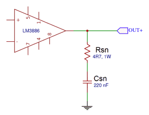
The Zobel network is used to prevent oscillations caused by inductive loads. It also prevents radio frequencies picked up by the speaker wires from getting back into the amplifier’s inverting input via the feedback loop.
At high frequencies, the impedance of Csn is very low, so high frequency current is shorted to ground. Rsn limits the high frequency current so there isn’t a direct short to ground, which could exceed the current limit of the LM3886. Therefore, smaller values of Rsn make the Zobel network more efficient at filtering radio frequencies, but it also increases the cutoff frequency, which in turn reduces it’s effectiveness.
The datasheet gives a value of 2.7 Ω for Rsn, and a value of 100 nF for Csn. This makes the Fc:
589 kHz is fairly high, especially since the lowest frequency of AM radio broadcast is 535 kHz. In order to bring this down to a more reasonable level, I decided on using 4.7 Ω for Rsn and 220 nF for Csn, which lowers the Fc down to 154 kHz:
154 kHz is well above the 20 kHz limit of human hearing, and well below any radio frequencies the speaker wires might pick up.
Since Rsn will need to shunt high currents to ground if the amplifier oscillates, the power rating should be at least 1 Watt. Csn should have low ESR and low ESL, with a voltage rating greater than the rail to rail swing of output voltage. To minimize inductance, locate the Zobel network close to the output pin (pin 4) and keep the traces short.
The Thiele Network
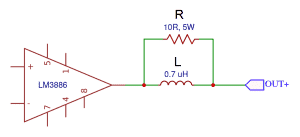
While the Zobel network reduces oscillations caused by inductive loads, the Thiele network reduces oscillations caused by capacitive loads, usually due to long speaker cables. It also prevents radio frequencies picked up by the speaker wires from getting back into the amplifier’s inverting input through the feedback loop.
Inductors have a low impedance to low frequency current and a high impedance to high frequency current. Audio signals are relatively low frequency, so they will flow through the inductor uninhibited. High frequency oscillation current will be impeded by the inductor and be forced to flow through the resistor, which will dampen it.
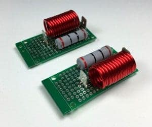
The datasheet recommends a 10 Ω, 5 Watt resistor in parallel with a 0.7 µH inductor. In a stereo amplifier, there will be one Thiele network per channel. They should be located away from the amplifier’s input circuitry to prevent interference from the magnetic fields generated by the inductor. A good location is near the speaker output terminals, separated a bit or at 90° angles to each other to prevent magnetic field coupling between them.
Making the Inductors
The inductors for the Thiele network are wire wound air core types, made by wrapping enamel coated wire (magnet wire) around a cylindrical object. Since the inductor will be carrying the full output current of the amplifier, the wire should be heavy gauge. 12 to 18 AWG would be good. Use this Single-Layer Air Coil Calculator to find out how many turns you need for a particular wire diameter and coil diameter.
Or you can calculate the inductance yourself with this formula:
I used 14 AWG magnet wire in my build since it’s thick and easy to find. The diameter of 14 AWG is 1.62814 mm. I planned on using a screwdriver shaft with a diameter of 11 mm to form the coil. Entering this information into the inductance calculator, I found I’d need about 12 wraps to get a 0.7 µH inductor.
Power Supply Decoupling Capacitors
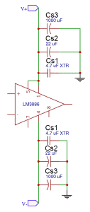
The LM3886 has one negative power supply pin (pin 4) and two positive power supply pins (pins 1 and 5). The negative supply pin needs it’s own set of decoupling capacitors and the positive supply pins share a separate set of decoupling capacitors.
The large decoupling capacitors provide a lasting source of reserve current when the low frequency output of the amplifier is high. Larger values will improve the bass response. Typical values are between 470 µF and 2200 µF.
The medium value decoupling capacitors supply extra current for mid-frequency output. These should be somewhere between 10 µF and 220 µF.
The small value decoupling capacitors provide current very quickly to help the amplifier output higher audio frequencies. They also filter noise and radio frequency interference in the power supply.
The decoupling capacitors also compensate for the parasitic inductance and resistance of the power supply wires and traces leading to the the chip’s power pins. Inductance and resistance inhibit the flow of current, which increases with longer wires and traces. Since the power supply is relatively far away from the chip, inductance and resistance are a problem. To maximize current flow to the chip, the decoupling capacitors should be placed as close as possible to the chip’s power pins.
Capacitors with lower equivalent series resistance (ESR) and lower equivalent series inductance (ESL) are the best types to use here.
Research by Tom Christiansen shows that a 4.7 µF ceramic X7R capacitor in parallel with a 22 µF electrolytic and 1000 µF electrolytic has significantly better performance than the paralleled 100 nF, 10 µF, and 470 µF capacitors recommended in the datasheet. That is what I’ll be using in my amplifier.
The Mute Circuit
Rm, Cm, and D1 form the mute circuit:
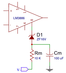
When the current flowing out of the mute pin (pin 8) is less than 0.5 mA, the amplifier’s output is muted, and when the current is greater than 0.5 mA, the output is un-muted.
To un-mute the amplifier, we need to find a value for Rm so that the current allowed to flow out of pin 8 is greater than 0.5 mA. That can be found with this formula:
For my amplifier running on a ±29.6 V supply voltage,
So, my Rm will need to be less than 54 kΩ for the current at pin 8 to be greater than 0.5 mA.
Rm and Cm create a time constant that slowly decreases the current at the mute pin when power to the amplifier is shut off, and slowly increases the current when the amp is turned on. The 16 V Zener diode (D1) blocks current flowing out of pin 8 until the diode’s breakdown voltage (16 V) has been reached. This produces a soft start/stop effect that gradually increases or decreases the volume instead of abruptly cutting it.
The time it takes the current to ramp up and down can be adjusted by changing the values of Rm or Cm according to the formula for the RC time constant:
For example, if I want a one second long soft start, I could arbitrarily set Rm to 10 kΩ, then find a value for Cm:
So setting Rm to 10 kΩ, and Cm to 100 µF will give me a one second long soft start.
The Final Schematic
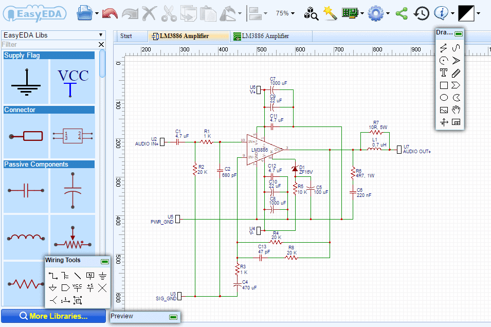
Now that we’ve seen how to calculate the component values, we can start designing the PCB layout and wiring scheme. If you don’t want do all of the calculations we did above, you can use the values I used. Here’s the final schematic:
Note: The component labels match the labels on the PCB layout provided below. Click on the image to edit the schematic or change component values.
Designing the Ground Layout
The ground layout of your amplifier has a major effect on sound quality. With a properly designed grounding layout, the amplifier’s output will be completely silent when the source is connected and no music is playing. With a poorly designed ground layout, the amplifier can produce a very noticeable hum or buzzing sound.
The key to a good grounding layout is to keep low current grounds separate from high current grounds. Low current grounds are the ground feeds to the input circuitry and feedback loop. High current grounds are the ground feeds to the power supply decoupling capacitors, the Zobel network, and the speakers. High currents flowing through the low current ground conductors will create a DC voltage that can show up at the amplifier’s input and get amplified as noise.
To separate the low current grounds from the high current grounds, we will create several ground networks:
- Audio input ground: Ground for the audio input cable
- Signal ground: Ground for the input circuitry – Rin, Cc, and Ri/Ci
- Speaker ground: Ground for the speakers
- Power ground: Ground for the power supply decoupling capacitors, Zobel network, mute capacitor, and the ground pin of the LM3886
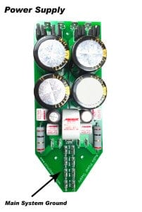
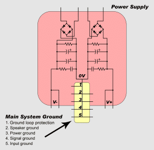
These grounds should connect only once at a set of terminals called the main system ground. The main system ground is located as close as possible the reservoir capacitors on the power supply. The main system ground will connect to the mains earth wire via a ground loop protection circuit (explained later), and the amplifier chassis.
The individual ground networks are connected to the main system ground so that higher current grounds are closer to the reservoir capacitors. The diagram below shows how to order the ground connections:
The speaker grounds and audio input grounds are routed directly from their terminals on the chassis to the main system ground.
Designing the PCB Layout
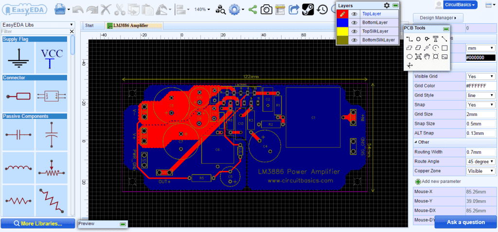
PCB design also has a major influence on the performance of your amplifier. Below I’ll discuss the guidelines I used to design this PCB layout. The PCB is for a single channel, so for a stereo amplifier, you’ll need to build two boards:
Note: The components on the PCB layout match the schematic above. You can click on the image above to edit the PCB layout, change the component footprints, and order PCB’s.
The PCB was designed with EasyEDA’s online design software. EasyEDA is a full suite schematic and PCB design software/manufacturing service that’s free to use and offers great prices on custom PCB manufacturing.
Ordering PCBs
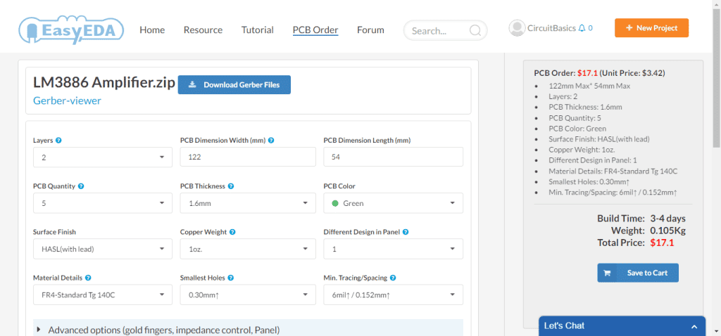
If you click on the “Fabrication Output” button in EasyEDA’s PCB editor, you’ll be taken to a page where you can order the PCB. You’ll be able to choose the copper thickness, PCB thickness, color, and order quantity:
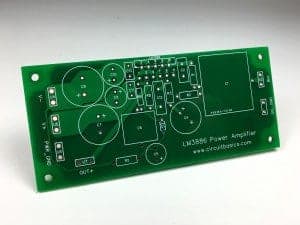
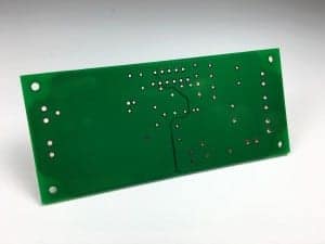
I ordered 5 boards for $17.10 USD and they were delivered in about 10 days. The finished boards look great. All of the traces and printing came out very clean and precise, and there were no defects on any of the boards. Here’s one of the PCBs:
PCB Design Guidelines
High currents flowing through the power supply and output traces will create magnetic fields that can generate currents in the feedback loop and input traces if they’re routed parallel to each other. This can distort the input signal, so it’s best to keep them far apart or route them at 90° angles. Placing their PCB terminals on opposite sides of the board will make it easier to keep them separate when you route the traces.
Any space between traces of the same circuit will create a loop that can transmit or receive electromagnetic fields. The traces for the power supply feeds and power ground should be routed close together to reduce the loop area. Likewise, the audio input and signal traces should be routed close to each other. An easy way to minimize the loop area is to use ground planes on the bottom layer of the PCB, which I’ve done in this layout.
The power ground and signal ground are the only ground networks on the PCB. Each one has its own electrically isolated ground plane on the bottom layer. Since the power ground carries high currents and the signal ground carries low currents, they’re kept separate until they connect at the main system ground. On the top layer of the PCB, the power supply, output, and Zobel network traces are routed over the power ground plane. The input and feedback loop traces are routed over the signal ground plane. The traces for the power supply feeds were made very wide to minimize the resistance and inductance.
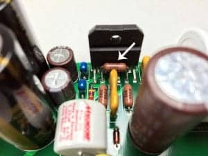
The feedback loop should be kept as short as possible to reduce the loop area. I trimmed the leads of the feedback resistor (Rf1) and soldered it directly to pins 9 and 3 to keep the loop area as small as possible:
Inductance inhibits the flow of current and creates resonance with a capacitor that’s in series. Since inductance increases with trace length, it’s best to keep all traces as short as possible. This is especially important for the power supply decoupling capacitors, feedback loop, input circuitry, and Zobel network. Keep the components for these circuits right up against the chip’s pins so the traces will be short.
We have more tips and tricks on designing PCBs in our How to Make a Custom PCB article, so check that out if you’re interested.
Wiring it All Together
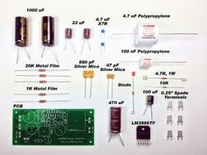
The LM3886 is a Hi-Fi chip amp, so I used high quality audio grade components for my amplifier:
The total cost came to about $118 for both channels, not including the chassis, power supply, and wiring parts. You can build it for a lot less with cheaper components if you’re on a budget, just be sure to change the component footprints in the PCB layout.
Solder and Soldering
Before soldering the components to the PCB, use a piece of fine grit sandpaper to remove any oxidation from the component leads. This will give you a stronger solder joint and better electrical conductivity.
To hold individual components in place while soldering, use a putty like Sticky-Tac on the top side of the PCB. Start soldering the smallest components first, and work your way up to the larger components.
Try to avoid the standard 60/40 tin lead solder and use a 63/37 eutectic solder instead. 60/40 solder has a wide melting range, and when it’s at the lower end of the range it becomes pasty. If the component moves in the pasty phase, it can create a cold solder joint. The smaller melting range of eutectic solder makes the solder set faster and gives a better electrical connection.
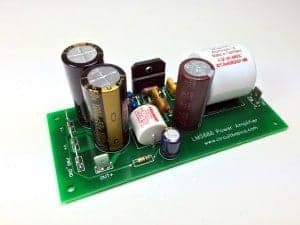
Here’s one channel of my amplifier after I soldered the components:
Finding a Chassis
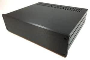
You’ll need an enclosure to keep the PCBs and wires contained and to mount the input, output, and power connectors. Metal enclosures are the best type because they shield the amplifier from interference caused by fluorescent lights, radios, and cell phones. Unfortunately it can be hard to find a chassis that fits everything and looks nice too. After a lot of searching, I found a company called Hi-Fi 2000 that manufactures some really nice metal enclosures. Their website is in Italian, but it can be translated to English. I ordered their 330×280 mm Galaxy model with a 10 mm black anodized aluminum front panel and it looks great:
They also do custom drilling and printing, so I had them customize the back panel:
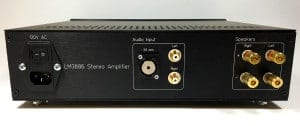
Before you order a chassis, do a test layout of the transformer, power supply, amplifier PCBs, and heat sinks. Then measure the overall dimensions to make sure the enclosure will fit everything.
Wiring Layout Inside the Chassis
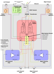
After the PCBs have been assembled and you have a chassis, it’s time to wire everything together. The wiring layout is just as important as the PCB layout and grounding layout. Use the diagram below as a guide for wiring the various parts together:
Click on the image to view a larger version.
The goal with wiring is to reduce or eliminate electromagnetic interference between high current and low current wires. The audio input wires and signal ground wires are the most sensitive to interference from surrounding magnetic fields.
The power supply wires, speaker output wires, transformer, rectifier diodes, and AC mains wires are a major source of magnetic fields. To reduce interference, keep the audio input and signal ground wires away from these parts or run them at 90° angles if separating them is unavoidable. If you orient the input side of the amplifier PCBs near the input terminals on the chassis, the wires can be kept short and away from sources of interference.
Any space between the wires of the same circuit will create a loop that can transmit or receive electromagnetic fields. To minimize the loop area, the following sets of wires should be twisted together tightly:
- Hot and neutral AC mains wires from the input terminal to the transformer
- AC zero and secondary voltage wires from the transformer to the power supply
- V+, V-, and power ground wires from the power supply to each amplifier PCB
- Speaker output and speaker ground wires from the amplifier PCB/main system ground to the chassis terminals
- Audio input and input ground wires from the input terminals to the amplifier PCBs
Three power supply wires (V+, V-, and power ground) connect the power supply’s DC output to each amplifier PCB. These wires should be thick, as short as possible, and twisted together tightly. I used 14 AWG, but anything larger than 18 AWG should be fine.
Only low currents flow through the input wires and signal ground wires, so they don’t need to be heavy gauge. I used solid core 22 AWG, which works well because it can be twisted into a tight coil.
Audio input cables running from the source to the amplifier chassis can pick up interference. If this becomes a problem, you can install a 1 nF capacitor between each input terminal ground and the chassis to filter it.
The mains earth wire should be secured directly to the chassis with a bolt and ring terminal. I’d also use a lock nut or lock washer to prevent it from getting loose. All metal parts of the amplifier (like the heat sinks) should be electrically connected to the chassis to provide a path to earth for any mains voltages that could contact them in the event of a fault.
The main system ground connects to the ground protection circuit (discussed below), which then connects to the chassis. The ground protection circuit can connect to the chassis at the bolt where the mains earth wire is connected to the chassis, or at a separate location.
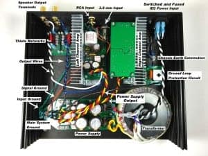
The two Thiele networks are located close to the speaker output terminals. To prevent interference between the inductors, they should be spaced apart or oriented at 90° angles to each other.
Here’s how I installed everything inside my chassis. The right channel PCB is mounted upside down so that the input side of the board is close to the RCA and 3.5 mm input terminals. In this arrangement, the heat sinks provide some shielding from the Thiele networks and the AC wires leading to the transformer:
Click on the image to view a larger version.
The Ground Loop Protection Circuit
GROUND LOOP PROTECTION CIRCUITS MAY BE ILLEGAL IN SOME AREAS. PLEASE CHECK YOUR LOCAL ELECTRICAL CODE OR CONSULT AN ELECTRICIAN BEFORE INSTALLING THIS…
When you connect a powered audio source to your amplifier, magnetic fields from the source’s transformer and power supply wires can be coupled into the ground wires of the audio input cables. This is know as a ground loop, and it can create hum in your amplifier’s output.
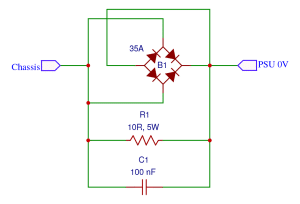
A ground loop protection circuit will break the ground loop current:
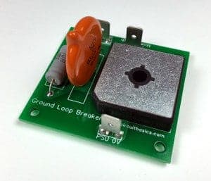
Under normal operating conditions, low voltage ground loop currents flow through the resistor (R1) to earth (the chassis). The resistor reduces this current and breaks the ground loop. If a high current fault occurs, the fault current can flow through the diode bridge to earth. Note that the chassis MUST be electrically connected to the mains earth wire to prevent mains voltages on the metal chassis in the event of a fault. The capacitor is there to filter any radio frequencies picked up by the chassis.
If a ground loop protection circuit is used, all input and output terminals must be electrically isolated from the chassis. Otherwise, the ground loop protection circuit will be bypassed entirely by the input/output ground wires that connect to the main system ground.
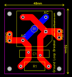
The ground loop protection circuit can be hard wired, but it’s a little neater to mount the components on a PCB. The “PSU 0V” terminal connects to the main system ground. The “Chassis” terminal connects to the chassis:
Click on the image to edit the layout, change component footprints, and order the PCB.
How Does it Sound?
The amplifier I built sounds incredibly good. It’s the best amp I’ve ever owned by far. The bass is very deep and clean. You can really feel it. The highs are clear, but not harsh at all. I can hear details in songs that I never knew were there. Trust me, if you build an amp with the LM3886 you will not be disappointed. It definitely lives up to it’s reputation as a Hi-Fi amplifier. The video at the beginning of the post will give you an idea of what it sounds like.
This should about cover most of what you’ll need to build an excellent sounding Hi-Fi amplifier with the LM3886. Due to the length of this post, I decided not to cover the power supply in detail, but I may do so in the future.
If you’re interested in building other amplifiers, we also have a tutorial on making a 25 Watt amplifier with the TDA2050, and making 10 Watt stereo and bridged amplifiers with the TDA2003 as well.
Thanks for reading… If you have any questions on this build, be sure to leave it in the comments below and we’ll try to answer it. And be sure to like, share, and subscribe if you found this helpful! Talk to you next time…






I use the LM3886 on my biamped mains. A single chip for each tweeter and a parallel pair for the woofers. This setup drives them quite well.
Hi Georg. I am interested in buying two amplifier plates and one power supply. I am asking for information by email desoto100@wp.pl
Can u provide me circuit diagram of parallel pair chip ?? What output power will it give
Thnx..
Hey, great job! thanks for sharing. Cant wait to see post on power supply!
Great post and well explained. If possible please post on Power Supply, Speaker Protection, Soft Start and Pre-Amp.
Thanks…………..
Love the post. Great detail and explanations of the individual aspects of the circuit. I also really like how you supplied the calculations for determining the size of the components. As others have stated, I’d love to see a followup on the power supply. If not a full post cover it, could you at a minimum post a link to the pcb?
Thanks!
Great job, very well explained. Thanks
I enjoyed every moment of the explanation, Great work and thank you for sharing
everything were very well explained. thanks for sharing.
Thank you very much for your detailed explanation, I”m searching for the same.
Great project; thank you for sharing. The LM3886 is an excellent component and you explained “who to do better”.
Thank you for sharing this.
Shouldn’t you also consider the voltage drop on the rectifier diodes, when you calculate the maximum voltage required by the amplifier?
thanks.
I was wondering the same thing. I think this is an omission in the article. Depending on the rectifier and diodes used, this should be anywhere from 1.1V – 1.4V subtracted from the transformer output voltage.
Thank you for this really great article.
Do you think you could post the exhaustive list, brandd and referenced of the components ?
thanks.
Nice work! I wish I had had this guide years ago when I first tried building an LM3886 amp. I second the request for component details, such as the voltages of the caps that can’t be read, if possible.
Thanks. The best article ever. I learn a lot, specially about grounding.
The best post I’ve ever seen on LM3886. Congratulations! A complete schematic, as well as components values for the power supply will be greatly appreciated, Thank you so much in advance.
Thanks for the explanation. I have a question though, if you said your amp will need +-30V, why would a +-18V transformer be enough?
The transformer only outputs AC, so the 18V rating is AC voltage. The amp needs about +-30V DC though. When you convert the transformer’s AC voltage to DC on the power supply, the voltage actually increases to about 25V due to the bridge rectifier.
Great article! Would it be possible to provide the PS schematic or the gerber files for the PCB board?
Thanks
Would be awesome to have links to getting the chosen audio components too.
Beautiful job. Congratulations and thanks for the details.
Top quality work.
True nice complete job! (y)
Thank you for sharing this documented design guide for LM3886.
A request .Could you also consider doing a solid state discrete power amp with dual dc power supply.
A pre-amp with tone controls would be also be a welcome.
There are many circuits on the net but again they do not explain any design aspects completely.
Kindly reach me
A very nice explanation. A lot of effort obviously went into this. Many thanks! Many thanks too for the fantastic links.
You seem to know what you are doing as well as having a lot of experience. Thus, I was wondering if you could state the specifications of your amp, (distortion and noise characteristics) so it can be compared to other LM3886 designs, so see if one needs to improve anything.
Also, I would try to slide the capacitors away from the heatsink more on the PCB design so that the modules would have a longer life in many years time before breakdowns.
How come you amp isn’t picking up hum or the local AM radio station when its not in a shielded box?
Crazy input capacitor!
Great post!!!!
Thanks.
Just a question: if I want to use a volume control, how should I set the input resistor to limit dc offset due to input bias current?
thank you so much for your posting of the parts list as well as the power supply schematic and values!!
Thanks a lot for sharing this wonderful job. I will definetly try a build on my own.
Sascha
Awesome writeup, many thanks! Quick question, I’m making these amplifiers to work in my car, so I will be using a 12V-30V DC transformer to power it. Should I still include a ground loop protection circuit or is it not needed for this approach?
no comment, just want to follow this very nice thread!
I don’t know if I am misreading your schematic but it appears that your board silkscreen is mislabeled. The two silver mica capacitors (47pF and 680pF) appear to be reversed in your pictures. the footprint size of the components appears to be reversed if C2 sets the high frequency roll off of the amplifier then this would be the 680pF capacitor (the lager of the two) this is reflected in the picture of your components laid out with labels.
As C13 is used to stabilize the amplifier I would just like confirmation that the parts list and silkscreen are correct. Thank you.
Hi Darren,
I see that on the photograph of the parts family, the names of the two mica C’s are reversed.. The 680 is in fact the smaller-, the 47pF is the bigger one!
So the silkscreen is correct….
Success with the build,
Ed
Hi, friend,
I´ve got the PCB but when I started to put the components , I didn´t find the holes for R4. Did you forget it?
I have a transformer that feeds 22V at 7A.. I can use it, no?
Hi José,
You are supposed to place R4 (20 Ohm) between pins 3 and 9 directly ON the chip.
Good luck,
Ed
Best tutorial you’ve ever made and one of the best available online. I hope you’ll make more of those overly detailed explanations, amazing knowledge source.
First off – thank you for the great tutorial and the breakdown of each step. As an electrical engineering student, I love getting the chance to truly understand the process of creating the design.
Second, I’m trying to design the amp to go with a pair of Bose Interaudio 4000 speakers, which have a rating of 10-100W and 4-8 ohms. Since they do not have a specific value, but instead a range, should I make the calculations using the higher values, as a worst case scenario or sorts?
Thanks for the help!
Wow, best guide about building LM3886 amplifier. I would not call this basics. There are many deep understandings beneath the guide. I like the way you treat ground connections. But I think three wire transformer output should also do just fine. I would like a kit to same the time to order them. I do not care particular brands of capacitors or any other components as long as their specs meet requirements.
Excellent post! I would like to ask some questions. Firstly , if we want a volume control for this amplifier, how we will achieve it?
Second is there any need for preamp as my audio source would be a laptop or a smatphone.
Although your question is a year old, I will answer it with my assumptions so far after searching online with the same questions in mind. Maybe it helps other people with similar questions. Please double check the information below, as I do not have alot of knowledge about electronics yet (I am a newbie).
If you look up page 7 in the LM1036 document below, you will find a schematic for tone/bass/treble/volume controls for stereo amplifiers. You can add an input selector knob (if you want more inputs) on the same controls-pcb and then mount the pcb parallel to where your control knobs should be. Most of the time the controls pcb will be mounted parallel towards the front of the amplifier. Most designs have extensionrods are used between the pcb and the controlknobs at the front, to obtain a better internal layout. You do not want wires going from the back to the front of the amplifier and back again, so power components and pcb’s in the front half of the amplifier and signal pcb’s and components in the back is optimal imho. My assumption is that how more “stuff” you add between the signal-input and amplified output circuit, the more distortion you could get (seems logical). Simply adding “some controls” could decrease/alter the sound quality output, or not. If you want to add controls to your amplifier, design your controlscircuit of similar high quality as the (munford) components and circuit designs used.
http://www.learnabout-electronics.org/Downloads/lm1036-Tone%20control%20IC.pdf
Imho not adding controls is a good idea if you already have a control on your sound producing devices connected to this amplifier. I.e. for your computer you can simply download some freeware controlssoftware to alter the input signal of your amplier. This because having 2 control options is redundant, this way the amplifier can provide the highest soundquality possible (because it has less parts to distort/alter the signal). But if you still want controls-knobs like I do, then researching in which way a controlscircuit is less likely to decrease/alter the soundquality could be the way to go from here. Like, I am going to try to design a controlscircuit for this diy amplifier project, that I can add later on in the case as an upgrade, before I start building this diy amplifier project for real.
Hopefully my reply helps, if not… whatever. ;-)
Hello , this is a real complete guide for building a high quality amplifier. However I am almost a new graduate of Electrical Engineer and not sure if I can handle the processes. Anyone has any idea on how to be qualified in order to build this amplifier without major mistakes ? Thank you in advance.
Hello Circuit Basics. I really enjoyed reading this awesome guide! I would like to know if there is a way to buy the power supply PCB instead of making it from scratch. Thank you.
Hi, I really enjoyed reading this ! I don’t have the patience to start this project can you advise me on where to find a really good lm3886 assembled board. also have an 8 ohm load and looking for Lm board with at least 80w/ channel.
Thanks again,
Rob nyc
Congratulations for the excellent post!
I assembled the circuit exactly like the one in the guide, with the following changes in the PSU: 24-0-24 250 VA transformer and 4x 10000 uf 50V, having + -32.8 volts dc. In the rest everything is equal to the circuit. The sound is fantastic, however I can not reach it but the power is far from expected. What could be wrong?
Can you help please.
Thank you.
Nheco
Thank you for your excellent work on this guide. I think you’ve completed the most comprehensive and understandable post on this subject. I can’t thank you enough.
Hi! This is _really_ a fantastic guide for a newbie like myself. I would also like to see a follow up post with details on the power supply. And I have a few questions:
Is there any reason why the input capacitor C1 has such a huge voltage rating well above the theoretical maximum of 60.4V from the positive to the negative rail of the power supply? Or is it just because the part is only manufactured like that by Mundorf?
If the latter: Are there any benefits (audio signal quality or other reason) with axial capacitors with such big plates? I was thinking of using one of the smaller WIMA MKP 4 series capacitors for C1. Those are also metalized polypropylene film capacitors, but with a smaller footprint and lower voltage ratings. The drawback is a bigger tolerance (10%), but they are dirt cheap compared to the Mundorf monster cap used here (WIMA MKP4F044706F00KSSD is about 1/7 of the price and way easier to find where I live).
And lastly a tip/request/suggestion for your CSS:
Could you please add a print stylesheet to the website, where all the unnecessary stuff (navigation, newsletter subsciption, social links, footer, etc) is hidden and the content column has full width?
Also, older versions of Firefox have problems when parts of the page are not “display: block”. On this web site it’s the #content-area DIV that is set to “display: flex”, that causes Firefox to print only the header on the first page, then whatever part of the article fits on the second page, followed by third page with just the footer. All other (47) pages of the article and the comments are hidden.
You could even add a DIV at the top of the web page with a .print-only class attribute, that is invisible when the page is viewed on a screen/tv, but would be included in the printed version. In there you could put things like a publishing date and a copyright notice, keywords, a table of contents, (social link) URLs written in full as normal text instead of just blue words in the article, etc.
I made an amp with LM3876 in 2015. From then on, I have been trying to improve its performance by making modifications. In addition, I wanted to publish a systematic article with instructions on that. However, due to lack of deep knowledge in electronics, the project was lagging behind.
Surprisingly, while searching for “Negative Feedback” of amps, I came here. This is amazing. Though I have no expertise in Physics, was able to understand the technical things in this article. This is far far better than I wanted to publish, or would say – THE BEST. Awesome job, guys.
Thanks for all the hard work. I noticed that in the schematic you have a 100nF cap (Csn). And in the photo under Wiring It All Together, there is a polypropylene cap labelled as a 100nF cap (I assume this is Csn). You explain in the tutorial (and as the actual photo of the cap shows) the actual value of the polypropylene is .22uF. Could you update this info. Thanks.
Thanks a lot for this awesome project. This is my first and through the detailed explanation, I’m well able to understand almost all of it.
I have a question though. For the power supply circuit, how can I connect diodes and capacitors to safely give the required voltage and do away with the transformer.
Thanks in advance.
Hi.
Some designs used only these parts For input:
1-Rb and Rin
2-Cim,Rb,Rin
3-Rb,Rin,Cc
4-Cin,Rin,Rb,Cc
Is there any order we should follow?
Rb before Rin or Rin before Rb?
Cin after Rin?
Cc before Rb?
Cc before or after Cin?
Can I use Cin and Cc in The between of Rin and Rc?…….
Thanks.
Thank you for posting.
Very similar to Neurochrome design procedure, except Neurochrome uses Crest factor for RMS Power.
Possible options:
Use two smaller transformers and put bridge and caps on amplifier board. Use low ESR bulk storage caps and minimize inductance lengths. Keep all unregulated storage caps close to the LM3886 with proximity based on parasitic inductance effects. Meaning, small caps closest to LM3886. The combination of bulk caps should provide low impedance current throughout the frequency band for the load. Also, at the same time provide IC centric decoupling of the supply.
Heat sinks for Natural Convection should be exposed to room air flow. However If amp is run at near full load (not likely) heating effects of the transformer and bulk storage caps should be cooled as well. (This is where you find air flow holes across the entire top and bottom of enclosure.) Use the metal tab version of the part. Published Rth of plastic is optimistic.
Weakest link: Supply large bulk storage caps. The design should specify based on cap heating RMS Ripple current effects (ESR), which basically translate into Capacitor life expectancy. So depending on the capacitor supplier used, the design may have larger bulk capacitance, divided into multiple smaller caps in parallel as needed that can satisfy the RMS ripple requirement. Also, some airflow spacing is needed around the caps.
Hope the above was helpful.
Absolutely top-notch. A person with or without electronics knowledge can follow this quite easily. This helped me have the courage to continue with my own Gainclone amp project. THANK YOU.
Fantastic tutorial. It explained so much.
Truly fantastic stuff you got here! I just finished my build based on your tutorial, with minor changes. I used single sided PCB, but tried sticking to your layout as closely as possible and changed some components – especially the Mundorfs for something readily available (and a bit cheaper ;) ). When I powered it up it sounded… different. At least to me, but I’ve been listening only to Yamahas for the past 10 plus years. Now after a couple of hours of listening to the LM3886 I must say it really sounds great! But it wasn’t so from the start – either I wasn’t used to the sound or the amp needs some time to burn in (which many people say is a myth). At first, the sound stage seemed too narrow to me and some of the songs sounded somehow odd – mostly metal tunes, in some the mids sounded somehow hollow. I think the sound my LM3886 amp produces is much sweeter and softer than my Yamaha. That’s why death metal sounds… odd :D. Also the imaging and mids either improved quite a bit in time or I just wasn’t paying attention at first. But I was astounded. I listened to songs I heard hundreds of times with a slack jaw. Amazing! Also, due to the sweeter and softer nature of the sound I’m able to comfortably listen to it on a volume which I would hardly stand listening to on the Yamaha.
I will add a comment to this post: I calculated the total cost of accuiring these exact components in The Netherlands (europe): €80 (mouser) + €180 (hificollective) + €120 (modushop enclosure including heatsinks) + €50 (ebay/amazon/other) = €430,– in total without pcb’s. If someone wants to add tonecontrols, I think you should atleast think about €125– in total for components+pcb+knobs+rods+fasteners+aluminium profile+etc is my assumption.
Hi,
Excellent work.. Love the in depth circuit analysis on components functions and why values were selected.
I would like to know how much the project costs for a stereo system including the power supply/transformer and where can i order these modules/accessories?
I live in Manila, Philippines.
Best regards.
Wery nice article! Thanks a lot! Only one thing- why the pcb ordering link won’t work anymore?
Chip amps sound mediocre
Oops! I get no sound out of the amplifier and it’s something I can’t figure out on my own. :( when I connect a power supply (tried 2 different ones), voltage slowly rises on both the positive and the negative rail on all power supplies on both channels with no signal through the speakers. Any idea what it can be?
Make sure you haven’t got fake chips! Get from a reputable supplier (components specialists rather than ebay).
Thanks for your reply, Robin! I sure hope I got genuine chips as I ordered them from Mouser.
Funny thing is: my LM3886 amplifiers from AliExpress and eBay are both working fine. Pretty ironic.
I recently discovered a couple of bad solder joints on the new ones, so there’s a *ahum* “slight” possibility that might have something to do with it… Looks like I have something to do for the weekend.
I signed up for the partslist but I am not recieving any partslists, can someone upload the partslist, thank you.
Sorry to hear that… Try checking your spam folder. If it’s not there, then send us a message through our comment form and we’ll make sure you get it:
https://www.circuitbasics.com/contact-us/
Thank you!
Hi guys! Can I ask?
I found the post about LM3886 amplifier.
https://www.circuitbasics.com/design-hi-fi-audio…/
In this post the author writes about Iphone as input signal source with 1 volt lvl. I want to use PC’s intagrated Realtek sound card as signal source. Which voltage level gives this output? Probably 1 volt too?
Thank you in advance!
Your LM3886 article is fantastic. It just does not get better than that! However , is it possible to go directly to EDA with info you posted for the amplifier board? Do they have any kind of records on that so it may only require a push of a button on this end?
Robert
Great article, thanks a lot. Could you explain briefly, the advantages/disadvantages of the T versus TF versions of the LM3886? You use the TF version, why is that? Thanks.
John- in regards to the case, the T version is non isolated meaning the back of the case is clean metal connected directly to the -V supply which requires electrically insulating it from the heat sink. The TF version is isolated and mounts directly to the heat sink. The thermal resistance of the TF version plus thermal paste is about 2.2 C/ case to sink.The thermal resistance of the T version including mica insulator and paste is about 1.4C/W case to sink. Although its a bit more work, I prefer the T version for the 0.8 C/W increase over the other. This allows for a smaller heat sink for the required dissipation thus saving a considerable amount of space and cost.
Robert
Robert
Thank you very much for the reply. You explained it very well to me!
All the best
John
Thanks a million for the detailed top quality guidance. It is hard to resist from building this amp:-)
A question: If a separate supply is provided for each channel (with separate capacitors bank for each channel, or even possibly with two power transformers), how should grounding be organized? With two two separate power supply units, all grounds be channel specific on the PCBs and the two ground-loop protection circuits (one from each power supply unit PCB) connected together to the chassis?
Thank you.
Thank you for your excellent work! I have just a question: in section “SET THE LOW FREQUENCY CUTOFF AT THE FEEDBACK LOOP”, how did you obtain the formula for Ci ? I would like to better understand how to set a value for low-frequency cutoff at the feedback loop. Thanks in advance.
Your efforts really appreciated….thanks a lot
Hi All,
someone correct me if I am wrong, the photo showing the board shows the 680pf in place of the 50pf as is the board lay out.
From my understanding the 50pf should be C13 and the 680pf the C2??
that had me confused for a while because of the pcb layout and the image.
Anyone?
If I am correct the pcb layout needs to be modified to represent the difference in size between the 50pf and the 680pf
all the best
Hi all
my 51pf silver mica is definitely much smaller than the 615pf silver mica I have so….?
thanks in advance for any clarification but the 615pf definitely goes to ground,
khurrum
To all
this really is the best site for anyone considering building a Gainclone
For me it has been invaluable in “gaining” essential knowledge towards the building of a gainclone.
My suggestion would be to not just follow the instructions, which are very well explained, but to take full advantage of the instructions as a starting point to a better understanding of exactly what each component is doing.
The means to do so have been provided.
all the best khurrum
I have built a couple of the Peter Daniels Audiosector Gainclones before.
Both the lm3875 and the lm4780 which are both very impressive.
If I may offer my observations, which are purely subjective though based and no doubt influenced by research
The power supply and each of the individual components do have a massive influence, especially as there are so few of them.
Mono blocks, rather than stereo, the volume control before the amps, not in the amps, using a passive or a buffered pre-amp is essential for quality
The power supply is all important and IS a part of the signal path, it controls it
Bearing in mind most is subjective, though differences between components of different materials do have a definite measurable difference e.g carbon v metal film resistors, silver mica v polyprop capacitors etc.
With the knowledge and the tools available on this site I have built very modified boards. 10 minimum so… 2oz copper
They have ended up 250mm x 170mm and the board is a z shape and the pins etc allow me to swap the various components (polystyrene caps are massive) I have connected some components underneath and supported them on separate boards
the holes have been kept as small a diameter as possible so the component pins need a light sand and pull through to fit through, maximum contact without solder, keys the pins as well.
Soldering quality does make a noticeable difference, don’t bend pins at the body, will cause damage
I have sourced components from ebay from Russia and the Ukraine.
Military grade Silver Mica capacitors SSG2 0.1uf at 0.3% tolerance (possibly the best capacitor made)
615pf at 0.3% tolerance
FT3 teflon 0.47uf and 0.22uf and 680pf
Polystyrene 4uf, 1uf, 0.22uf and 680pf and 48pf
All at amazing prices when compared to what they would cost here if obtainable without custom order.
From the left
I’ve moved the 4.7uf ceramic onto the pins, bottom of board obviously
used 2x10uf polyester mounted both sides of board for mids.
used 220uf then 3x470uf bipolar nichicon 50v electrolytics
Power ground is between V+ and V-
2 currents flowing in same direction will have cross interference due to proximity, ideally should be at 90 degrees or have sufficient space
2×0.1uf silver mica for rf oscillation filter, sm is the best followed very closely by polystyrene. noticable difference from polyprop, (I know?the rf oscillation fiter makes a difference) hmmm, could be subjective
signal in paralleled 0.2uf silver mica, 1uf teflon and 4uf polystyrene
signal shunt to ground paralleled 0.2uf silver mica, 1uf teflon, 3uf polypropylene, 30uf polypropylene 100uf bi-polar nichicon 63v and 330uf nichicon b.p
Seems counter productive to use film cap on signal in, then electro for shunt
From my understanding re: “bypassing capacitors”
for power supply decoupling the values are dependent on frequency requirements
for signal path coupling should be at least 10% of next capacitor value so; 0.1uf, 1uf, 10uf, the reason for the 3uf polypropylene above, to link the 0.47 teflon to the 30uf polyprop
using tiny values as mentioned in some forums, produces nothing noticeable , at least not to my ears
used 5ppm 22k vishay resistors on signal path and 22k holco 15ppm on some boards
income 22k uses 4 x the voltage so gets warmer so important to have close ppm
15ppm 21k holco for balance bias current resistors and 15ppm holco everywhere else.
A bit much perhaps? the difference in price is negligible
The board layout has allowed for flexibility which will allow for experimenting with components.
Every component really does make a noticeable difference
choice is subjective for example;
it seems people like the foil in oil because the oil allows movement which causes distortion in 2nd order harmonics, which people perceive as warm.
Too much clarity is not something people are used to, which can be an issue
still experimenting
Oh! all a bit pointless without sensitive speakers to match.
I have built 98db sensitive speakers, without physically large speakers it’s a little difficult to achieve sensitivity
That is another subject altogether, all I will say is that the vast majority of commercial speakers have just been thrown together more or less. Crossed over at 1000 and 7000, that’s about it
No matching of different drivers resonance frequency etc then crossover to match
It is definitely worth building ones own speaker system using a dsp rather than a cross-over, same as the Gainclones one can have exceptional performance at a fraction of the cost if one is willing to put in the time and study
I am now in the process of building 3 way active speakers, initially with crossovers then with dsp’s fed through a preamp.
The advantages of the amps in the speakers are immense and save on cost of cases binding posts banana plugs length of wire etc as well as massive improvement in audio quality.
I do believe a carefully planned lm3886 using quality (not expensive) components with suitable source, volume control feeding decent speakers is difficult to beat.
all the best
Hello!
Im considering building the amp, but i have a question that i sadly havent found an asnwer to. I have quite a bit of leftover CPU coolers and i have an idea to use those for building an amp based on 3886. So the question is, if and how much would adding fans to near the circuit affect sound quality? Obviously i would use 120mm+ fans on low rpm-s. But the question is if the motors operation would generate enough electric fields to start generating noise in the amplifier?
Regards
Marten
I’m confused. I ordered exactly the chassis and heatsink as specified and there is no way that the heatsink will fit in that chassis. The heatsink is huge. And now I am left with these choices.
1. Buy a bigger case.
2. Saw down the heatsìnk.
What have others done to resolve this ? Or did you order some other combination of heatsink and case ?
Whoa !!!
The PCB has 2 holes for the diodes, but the parts list specifies a 3 pin diode.
Whats up with that.
Im beginning to not trust this beast.
MUR860G vs MURF860G
Oops, my bad. The actual diode has only 2 posts rather than 3 as is shown in the data sheet.
Hi, i am confuse this is what we can read in your Guides,
for LM3886
“Audio input cables running from the source to the amplifier chassis can pick up interference. If this becomes a problem, you can install a 1 nF capacitor between each input terminal ground and the chassis to filter it”.
For TDA 2050:
“Audio input cables from the source can pick up stray electromagnetic interference. To filter this out, you can install a 1 nF capacitor at each input terminal, from the positive side to ground”.
which one is right?? from the positive to ground or from ground to chassis
Hi
love the design and want to build the amplifier
when I’m trying to order the PCB for the amplifier and the power supply from EasyEDA its running DRC tests and i get many errors ‘Pad to Copper Area’
i didn’t change the file just saved it
Is it OK to proceed?
Thanks,
Dan
Dan, I dont remember but I dont think so. If there were a way to trade email addresses, I think that I have a few of the amplifier boards in my shack. I could send them to you for the amount of the postage.
George KG5TKY
Hi George do you have still the LM3886 PCB left available? thanks.
Hi! I had the same, and i placed the order anyway. Package is still on ship. What to expect? Am i safe?
I am having a hard time finding X7R Ceramic resistors. Is there are substitte that can be used? Thanks a lot!
X7R ceramic resistors? Did you mean X7R ceramic capacitors. Commonly available through Moser and DigiKey.
Yup, meant a cap. I take may hat off to you Robert. Thanks!
Couple quick questions:
1) I am just starting to get into DIY audio and while this amp seems like a great quality amp and the article is very in depth I am wondering if this is too complicated for a first amp build?
2) with the above in mind I also don’t want to drop a fortune on a project I am going to likely make mistakes on. Does anyone have a rough cost of building this amp??
I just priced it, mostly through mouser, DIY coils and substituting Erse MPX caps for the Mundorf. It came out to just under $35 per side for the components, but you have to consider the costs for the boards and power supply. If I build this my transformer will be one scraped out from an old Audiosource amp.
I have about $180 into the completed unit with enclosure. I purchased almost all the parts as new with only a few parts from my “junk box”. I did build my own enclosure with about $25 in material and I cut back on the high priced input coupling capacitors to another high grade film type. The unit looks very professional and the performance is fantastic.
Where would i put in a stereo potentiometer for volume control
What is the rating for the fuse at the power switch ? I looked all over for it and cannot find it.
thanks
I started with a 3 amp Fast Blo and it immediately blew on the first startup due to inrush currents of the 40,000 ‘ lytics. No surprise there! I then switched to a 3 amp Slo Blo and every thing works fine. I really think 2 amp or 21/2 amp would work really well, but did not have them in stock at the time. Alternately, you could fuse the power supply rails (+30 vdc and – 30 vdc) with a pair of 21/2 fuses. There are two schools of thought here. First being to place fuse at bridge input, which will protect all power supply components. However the big lytics will continue to conduct until fully discharged and continue to do damage for faulty down stream components. Second is to place fuse at the output end of the lytics. This will give good protection to the actual amp circuit but will not blow for shorted bridges or lytics! Fusing both AC line input and power rails are the best but more work and expense.
Robert Reed
/
which heatsink was actually used ?
And your reply is rife with grammatical errors.
Let it go. I think many of the posters are from countries where English is not the primary language.
Many many thnx to share this ..
Pls make thesis on power supply too.
Thnx in advance
Very nice tutorial. I’m trying to understand the origin of the mathematical formulas. In the section REQUIRED TRANSFORMER POWER, I cannot understand where the pi factor comes from. Is it from the bridge rectifiers? In that cas, it should be 2/pi… can anybody help me with that%
Hi
Your Tutorial is very nice especially to our novice like me.
Really appreciate if you include your tutorials in TDA 7293/4 chips.
Thank you very much this blog is very helpful.
Regards,
odie
Hi,
A comparison with the TDA7294 should be interesting.
I’m going to make it.
your job is truly inspiring me so i have to do it.
I’ve already bought the pcb and the main electronics circuitry.
I’m just missing the mundorfs and the toroidal.
It will be the last big step but i need time to save some money.
Doing your maths, i should have a 2×19,34 volts/370 VA toroidal to get 68 watts. Is that right?
I asked to a local dealer to quote a toroidal with this values for me, would you be so kind to give me your opinion? Is it worth doing it or i should buy a 18×2/330VA ? Thank you for your suggestion
(4ohm load)
Well done for a great article.
The way you explained all the design papameters was very useful to me
Wonderfully and informatively written. I’ve learned a lot from your detailed sections on build and theory. Just about finished building the amp as described here. Future plans are (to try to) alter the amplifier PCB to use a Mundorf MCap Supreme Silver Oil instead the Evo Oil (an increase of about 44mm in length; 27mm to 71mm long). I’m still fumbling when trying my hand at using the EasyEDA software.
Hello
Is any one change to 8ohm
I think that only 25v DC will make it
Run to 8 ohm speakers
Yuval
Yuval, I built them amp just as described and I’m using it with my 8 ohm speakers. Sounds fine to me. I will, however, get a 330-400V 25+25 torroidal to see it it sounds any better.
Hello, have you try with the new transformer ? I have order the pcbs but no the components.
So if it works correctly for you, I take directly a 330-400V 25+25 transformer instead of the recommended one.
Thank you.
Arnaud, I’m actually using this one http://www.antekinc.com/as-4428-400va-28v-transformer/ . I’ve been trying to find the Avel Lindberg 330V 25+25 but no one has stock in the USA that I can see. I drive 8 ohm speakers so I wanted a bit more horsepower. To tell you the honest truth I can’t hear a big difference between the 18+18 and the 28+28 and the larger toroidal’s use doesn’t improve the bass response. It also adds a lot more weight to the assembled components in a chassis. I don’t listen at high volume levels to be honest. My opinions are based on listening judgements and not electronic measurements.
Okay, thank you.
I also plan to use a pair of 8 ohm speakers, so if everything works properly with a little more juice in the input I will start with a solution equivalent to yours.
I may try to make comparative measurements if I also find an 18+18 in my business.
I may try to make comparative measurements if I also find an 18+18 in my stuff. * (stupid corrector)
Arnaud, one advantage in using the 18+18 is you can use higher rated uF Caps (using 35V instead of 50V) in both the PS and the amp w/o having to worry about their diameter limits fitting on the boards.
Thanks for the detailed writeup.
Can you provide more details about your power supply circuit. Is that a CRC filter circuit? How did you calculate the values for these resistors and capacitors? Do you have a circuit diagram for this power supply? The circuit in the grounding diagram doesn’t seem to include all the components.
Thanks
Jesin..all the way at the beginning of the article is a yellow box that states “Bonus..download my parts list”. A pop up box asks for an email address. They will send you a pdf of the parts list and the power supply schematic + Gerber files.
I note your information regarding the lowest am broadcast frequencies in your country, and you quote the am band (medium wave). What happens to long waveband signals and very high power VLF signals like from time signal transmitters? How would this alter component values?
regards john
Hi,
It’s a great project and I really liked it. I’m wondering where we can add bass control and volume control in this
You can add these at the input to the amp. At the same time, you could install a balance control. Guess what- you now have the makings of a standard preamp. You can do this in two different ways- Build everything into the original amp housing or build the additional controls into a separate enclosure. If it were me, I would opt for a separate enclosure which would leave room for multiple input/output connections also. In either case you will probably want to incorporate a quad op-amp (TLO84) for buffering, gain .etc. The down side of the separate enclosure is it will require its own power supply, but you could add a DC jack on the power amp and tap off whatever power you need there, probably less than one watt. There are numerous designs for these circuits on the web.
So I built this gainclone LM3886 chip amp and I learn a lot from doing it. Like all the other, simple LM3886 or LM3875 gainclones I’ve built the soundstage was magnificent, airy and brought detail to the music I’ve never realized before with my regular amps & DAC combinations (nothing high end). However, the bottom was always missing to the music. Preamps couldn’t add it back in either. If you really want to build a satisfying LM3886 amp, look to the My_Ref FE Evo A (My Reference Fremen Edition Evolution A amp). It’s more complex and expensive to build (it uses SMDs that either you can buy already attached or you can solder them on yourself) but you will be just astounded with the music coming out of your speakers. Realistically. I needed to have learned many things from reading this article, and building this amp, before I tackled the My_Ref amp.
Pete, yes this gainclone was a great project to build and the detailed theory was very instructive. I am interested in the Fremen Edition Evolution A amp as well but cant seem to find a link to where you can order some boards.
Dave, I am not sure but you can try this Forum: https://www.diyaudio.com/forums/chip-amps/234032-my_ref-fremen-edition-build-thread-tutorial.html
Hicoco
Thanks Hicoco….Dave: you’ll have to join the diyaudio forum and then private Message (PM) Dario Fremen (ClaveFremen) about purchasing the boards directly from him in Italy. He sells them either blank or with the SMDs (surface mounted devices) already soldered in place (for an extra fee of course). There is also a new build-buy forum
https://www.diyaudio.com/forums/group-buys/330082-my_ref-fremen-edition-gb-13th-gb-6.html
that you can read through.
Hicoco’s link is a very long read but its best to start from page one and just hack your way through it to learn the variations the builds have taken. Dario is currently up to build 1.72 I believe.
Regards,
Pete
I built a similar amplifier using the Hi-Fi 2000 “Galaxy” enclosure.
The assembled panels of the enclosure are not electrically connected, but they should be to have a proper earthing of the chassis.
How did you obatin electrical continuity between the front, back, side, top and bottom panels?
Thanks for the nice tutorial and beautiful built.
Regards.
Rodolfo
hi
I have just finish the buikt
I put some changes in Powe supply
troidial 24 0 24 with 6 /8200uf nichicon
happy with outcome
thanks
Yuval Abadi
I have this pcb made, and there is no R4?!!!!
why is c5 a 63 volt cap that is really high is it necessary?
Garry, R4 (also called Rfi) is soldered directly onto pins 3&9 on the LM3886 chip. See page 38? of the build guide. Why a 63V cap (versus a 50V like everywhere else) is needed in the Mute Circuit I can’t answer. Cheers
thanks man. i am not sure how that will be done though. the pins on the chip are so close and also i dont see this in the video. it if i solder a resistor between those pins it would be awkwardly floating on top of the chip and i just dont see that done on any other builds.
Gary, optimally it should have been done before soldering the LM3886 onto the board (see the written guide above). The alternative is to solder it to those pins on the underside of the board now. The idea is to keep the resistor leads as short as possible. I did the “directly onto the chip” procedure.. it took patience
Interested circuitbasics
Hello,
Nice project, good explanations, etc.
But I dont understand why C4 (470µF) is a polarised cap.
In my understanding there schould be an non polarised Cap, because there should be
an symetrical Audio Signal, so this Cap would be about half the time wrong polarised.
Im thankful of an Answer if I missunderstand something.
Henning, if you read the “SET THE LOW FREQUENCY CUTOFF AT THE FEEDBACK LOOP” section the author does state that a non-polar polypropylene could be used but the size of such a cap would be huge so an electrolytic cap is substituted. Looking through Mouser for a non-polar cap (470uF 50V) turned up a Panasonic and a few Nichicons but I’m not sure they possess “good musicality” as some folks might say.you need in the music signal path. Doesn’t mean you can’t try one and see what it sounds like. Comments folks?
Actually you can create a non polarized cap by putting to polarized back to back, i.e. the negative leads tied together which is what I’m doing for my spin on this excellent reference design. The resulting capacitance is of course 1/2 of the rated of each cap so make sure to take that into consideration. You need to start looking at 1000uF values which is coincidentally the same value as the audio grade caps in the local power supply circuit.
I’m tweaking some of the filter values for personal; preference and adding a an Arduino Nano to the mix for relay controlled speaker connect / disconnect, basic gain control and thermal monitoring.. Next iteration will have more pre-amp functions including source select, volume and tone control, all done digitally.
Again my compliments to the chef for a really great write up.
Wow! great Project, well explained! Thank you circuit Basics for the Details in Explanation.
Questions About the transformer:
1 – what would be the effect of using a 18-0-18 transformer (not 0-18, + 0-18) and share the common 0 as ground?
2 – Since the power per channel would be about 40watts, why should the transformer be rated 300VA? Can’t one use a 120VA 18-0-18V transformer? would that have a negetive effect on the Output power?
Thanks a lot guys in advance for a response
Are you using a center tapped transformer for the power supply?
hi
my amp have high redio buzzzz
any one may sugest sultion?
I build the amp borad are same as sescribed here
the rectifier I use other design , 50% more capsitor
trodial transformer 25-0-25 (i use 8 ohm speakers)
the grounfg loop same but I put other capcitor value 200nf (I got one in my box)
my other amp on same spaker calble pre amp is quit
Hey i would like to buy this PCB but don’t know how to
Mario, you actually have to have them made. Drop me a private email (randommailboris@gmail.com) and I’ll try to send you understandable instructions.
Hi there,
This was a super useful detailed post and I’ve started trying to make the above circuit but with a few small changes. My plan is to power this DC i.e. off a car battery or portable battery, however I’m really confused as to how all the grounds are arranged in this scenario, can power ground and V- just be connected to each other? If not how should they be connected up?
Hey hey hey! Am in the process of reviewing all the details in this guide to get started shortly with my build. I am a total newb so I will take my time so I can fully understand what I am doing and why. Was an electrician in the Navy many moons ago so I am not afraid of this as a hobby and am fully “safety” oriented.
Right off the bat, I have a doubt/concern. My speakers are a pair of Micca MB42X. The impedance info on the speakers themselves as well as Micca’s website states “Impedance: 4-8 Ohms”. Should I use 4 Ohms as my base for the power calculations? Use 8 Ohms? Or average the impedance out at 6 Ohms?
I will be using the amp/speaker setup for near-field purposes (mostly music with some gaming). My source will be the computer motherboard loaded with the Realtek 1220A codec.
Any other suggestions or tips… are welcome.
Thanks in advance.
Hello Victor. Just a heads up from me regarding the build.
I have just finished my build and I noticed right away that I had massive crossover distortion with poor, crackling sound as a result.
It turned out after a week of troubleshooting that it was the zener diode in the mute circuit that was the reason for the distortion.
The distortion vanished when i shorted the diode with a piece of wire.
Have a nice build!
I have seen in many audio amplifier, that the inductor L is wounded on resistor R. why you placed both component separate ?
Pl. explain
Thanking You
You attached the chassis earth to the bottom plate of the case, but how are the top, front, sides and rear of the cases earthed?
Through screws that hold chassis together.
The screws are painted so do not make electrical contact. I have one of the cases used in this project and have tested for electrical connect between panels. No electrical contact exits.
Is anybody able to make an audio input switch for this amp? I’m new to this world and i’m not an engineer, i made my personal research on the web, and all i understood is that a ic switch (adg1636, adg854,adg884) is better than relay switch and rotary switch. I’m I right? Please be kind :-)
There are plenty of pre-built switching circuits of both types to be found on eBay. The downside to rotary switches is that the contacts get dirty over time and will need cleaning but all the circuitry is back on the board keeping the signal path short. Relay contacts sometimes get worn/coated over time but you’ll only be having pre-amplified signal going through (not like relays for speaker protection).
Thank you
You can look at this:
https://www.tindie.com/products/hicoco/audio-input-selector-switch-relay-module-board/
thank you. i made my own
https://easyeda.com/aleraco/ti-switch
Thank you! Don’t you think that it is not good to have 4 or more coils close to circuitry or it may be disregarded?
Does not matter, this is very silent when you change input, no hum, no noise….
Builders, just a note on two variations I’ve made to my build which, on my system, has led to sonic improvements and slightly simplified the build. The sound is now a little fuller at the bottom end than it was before with the proviso that I mostly listen to classical music and some better recordings of Folk & Blues. I’ve eliminated all the recommended decoupling caps and just used Nichicon FG 470uF 50V caps in C7&C8 while in the PS build I’ve used four Nichicon 12000uF 50V caps (LKS1H123MESB). I can’t hear a difference with the Thiele network in place or not, so I just left it off. The soundstage is still quite broad & airy but the bottom now seems a little richer.
I’m going to test the amp PCB build with other types of nichicon 470uF caps at C7&C8 as well as trying different brand caps at C5 to see how the sound changes. I’m also going to look at CDE 15000uF caps in the PS to see how that changes the sound. I’m not an advanced electronics guy so no oscilloscope graphs/comparisons are gonna get posted.
Cheers, Pete
Thanks, nice project and superb explanations!
I would like to use the amplifier board described here togheter with power supply section of an old kit from chipamp.com that I already have (schematic shown on the link below).
In this case what’s the best way to handle grounds?
Thanks in advance,
Simone
Simone: I tested my amp boards using the chipamp PS and everything works fine. The outputs from the +PGND and -PGND are combined along with both the PWR_GNDs from each of the amp boards and all are sent to earth ground on your AC input. Also sent to earth ground are the SIG_GND from each board, and all the common (-) lines from the RCA inputs & speaker outputs. I tested it all on a bench top so there was no common metal case joining the components.
Pete
PS schematic – https://drive.google.com/file/d/1pk3knK2XnM-miUWUE3pPuHc-KMmIOE6N/view
Link dead
Looks like there’s a new link to request the PS schematic … https://www.circuitbasics.com/design-hi-fi-audio-amplifier-lm3886 Go to the Yellow box that starts with “Bonus: download my parts list ” and click on the link for requesting the parts list. A new pop-up box appears to request the info.
Cheers, Pete
Simone: your other power supply should work fine. Follow the grounding scheme in “ WIRING LAYOUT INSIDE THE CHASSIS” section. There is no 1nF cap on the signal input lines that I can see in the actual build (unless I missed something during my builds of this). I have the same chipamp.com power supply so I’ll have to try it out now and see what happens.
Hi all,
I just build the amp and set it up. Unfortunately no sound comes out. I have checked the power supply (switch mode, +35/ 0 /-35 500 Watts) and it actually gets to the amp. The wires of power supply was connected one after the other i.e. the GND , then the -35, then the +35. I also checked to make sure that sound from my smartphone gets into the amp. The output is connected to a 6 Ohm loudspeaker.
Now I need help, on ideas and hints, on how to diagnose the possible fault in the amp. I would really appreciate any help before I take every component one after the other.
Thanks for replies
Jackson
Jackson, I’m not trying to be condescending here, but as a start did you combine SIG_GND, the (-) line from the input signal and the (-) line from speakers out and send them all to a common earth ground (some folk call this a star ground connection in your case)? Next you can check the voltages across the terminals of C7, C8, C9, C10, C11, & C12 to see if the lm3886 is getting power. You can check voltages directly at the pins on LM3886 itself (look to its data sheet for correct pins ). Is R4 soldered directly onto the lm3886 across pins 3&9?
Unfortunately we can post pictures here so a visual inspection can’t be done.
Hope this helps as a start.
Pete
Hi Pete,
Thanks for replying and giving me at least the first hints on where to start troubleshooting. I have the same ground for both signal input and output, signal ground, which is then connected at one point with the power ground. I have measured the voltages across the C7, C8, C9, C10, C11, & C12, and the all show the supply voltage of 35V. (and therefore also directly on the LM Pins), R4 was actually found somewhere in the middle of the board, but I have now removed it and soldered it across pins 3&9. The test however didn’t show any difference, i.e. no sound at the ouput. The zener Diode i used is 9.1V zener diode. Any further suggestions would be appreciated.
Thanks,
Jackson
Jackson:
Two things: short the D1 zener (jumper it) taking it out of the muring circuit. R5 should be a 10K (or something less than 58K) now, correct? Measure the mV output at the speaker out terminals. It should read <10mV DC. Check with live music with the speakers hooked up. If that works try setting up the Muting Circuit as designed in the original design, D1 = 16V zener diode, R5 = 10K resistor and C5 = 100uF 63V electrolytic. If that does not fix it, try bypassing the Thiele network . I’m hoping you didn’t ruin the LM3886 chips themselves. Check the solder joint at Pin 8 of the LM3886.
I’m not sure what you mean about you has R4 somewhere else on the board since there is No spot to mount it anywhere else on the board.
Pete
Hi Pete,
I’m glad to say that after shorting the Zener D1, I can now get sound at the output. With a loudspeaker connected, I get a very clear sound of any piece of music played from my smartphone. However when the input is not connected to my phone, there is a loud irritating humming noise at the output(speaker). I have just been testing only one board. The boards are designed by me using the schematics and instructions from this platform.
Could you suggest what could be causing the hum?
When I designed the boards, I placed R4 directly on the boards, That’s what I meant by somewhere else on the board (but now soldered on the LM3886)
I have not installed the Thiele network yet.
Next I am going to purchase the right zener diode and try it again.
Thanks for the support!
Jackson
most likely it’s a ground fault. you would need to run a ground wire from source to amp. and one from amp to receiver.
Yes, and in addition to John’s advice, I would ask you to specifically try grounding the (-) side I the signal input as well, if that was not implied in his response. A last resort is the use of a GLB (ground loop breaker) circuit as part of your grounding scheme.
Jackson, could you send me a picture of one of your blank & finished amp boards? I’d like to see what you designed.
Thanks, Pete
pznas@optonline.net
Sorry Jackson, I pushed the send button w/o answering your question about hum. The earth ground that comes from your wall outlet is key here. Try grounding all return (-) leads from inputs and speaker outputs as a start. Use a “star ground” design (look it up) since grounding to your chassis may or may not work correctly (painted surfaces sometimes don’t conduct or connect correctly for a universal case ground. If the hum is still there then add the power supply’s neutral to the ground as well. That’s a start. What kind of transformer are you using btw? Is it isolated from touching the case ?
Pete
No problem Pete.
Please have a look at the pics. The design is definitely not the best looking :-) , more so as I purposely made a design that should be small enough to have 2 PCBs on a 100mmx100mm board. For the hum issue, I’ll try the suggestions you listed above. However, as I mentioned before, the hum only exists when the input is left open (without any connection to it). My design is intended to be used with a bluetooth module, having the option to connect any bluetooth compatible device, has a radio receiver, an option for usb/SD card insertion as well as an AUX input. Ones the module is connected to the amp input, the hum vanishes, and I’m left with a very clear sound. All I need now is to assemble the second board and I am done with the stereo system. I actually plan to have the whole system installed in a wooden casing, would I still need a ground loop circuit?
For the power supply, I’m using a switch mode power supply (SMPS), +35V_0V_-35V 500W, and for the load I use a 6Ohm 100W speaker, summing up to a total of about 80W drawn from the amp, and it really sounds like 80W. The stereo should give me about 160W
Jackson
Jackson, i can’t really make it out but does the blocking side of you D1 have continuity with Pin 8 on the LM3886?
Earth ground the “0“ terminal of your switching PS as well. You’ll especially need a star ground configuration in a wooden case. You may have to ground each of the heatsinks as well.
Is your mains voltage calculation correct?
You seem to have calculated 10% of 110 as 1.1 when it should be 11?
Or have I misunderstood the calculations?
Thanks.
Tony, I think the author was using 1.1 as a factor in the calculation implying the mains voltage (=1) and adding 10% to it (10% of 1 is 0.1) hence the factor is 100% + 10% = 1.1. Actual voltage is only in the equation as V-transformer and in the results. Someone can correct me if I’m wrong here.
Cheers, Pete
Set the Low Frequency Cutoff at the Feedback Loop – the diagram under that title I think needs the 20k resistor between output and neg input. It’s in the later diagrams and there’s a 20k in the calculations.
Rich: I think the author only wanted to show the two components of the high pass filter in that diagram. The 20K resistor shows up in the “Stability Components Rf2 & Cf” section.
Pete
20K resistor is I think ok
Hi.. very interesting reading, enjoyed every moment of it. i`m really a new i the pcb design is it possible to get the cad file for pcb layout so i can order the pcb.. would really appreciate it
Jørgen: the gerber PCB files are referenced all the way at the beginning of the article. The production costs aren’t very high but the shipping costs are, unless you have a more local production facility.
Cheers,
Pete
Hi all
I’ve 5 pcb of each parts new , i won’t use them because of lack of time.
Send me mail at fredcab@gmail.com
Hi guys i need help.
i burned the 2 caps in 2 different times, the 22uF first, then i made a new board and the 1000uF blew.
i disconnected everything to check, and giving power just to the psu i have 50volts cc to the v+ v- terminals , on both channels (50 on L and 50 on R). this is unexpected to me because i was expecting to have 32 volts to feed the amp
my toroidal is a 18v/9A per channel
help please!
thank you!
Alessandro: which make & model number transformer do you have? If it’s a toroidal, it sounds like you wired the secondaries in series (doubling the rated voltage output ) rather than parallel (keeping rated voltage but doubling amperage) and once the 18+18V goes through the diode bridge rectifier circuit it would be 32 x 1.4 = 45V minimally. Usually the trans that is stated to be 18V runs a little higher, maybe 19-20V so 19+19V = 38V then times 1.4 = 53V.
Pete
Hi Pete!
It is a custom made tailored for my request of 18v/9A on two secondary plus a third secondary of 9v/3A.
I cant find the schema, but i can measure 18 v between grey/grey and 18 v between black/black. Grey/black gives 0 in any combination.
What can i do now? If there nothing to do with the toroidal, do you think i can change the voltage rating of the caps with success?
Thank you for your time!
Alessandro: first thing I would do is contact the person who made the granny for you and ask them the secondary output wiring as a confirmation. I’ll make the assumption it’s not a center-tapped transformer. Going with what you measured, disconnect the tranny + PS from the amp. If you built the PS as in this article then grey + grey goes to either VAC1 + OV1 or VAC2 + OV2 and black + black would go to the whichever set you didn’t use for the grey + grey. Using any of the GNDs out in the PS supply section of the board, what do you measure at both V+ & V-?
Pete
Tranny not Granny…sorry..my typing bad
Pete
V+(L) / GND L = 25v , V-(L)/GND L =-25v
V+(R)/GND= 25v, V-(R)/GND R= -25v
Ok, that sounds correct. So V+ (L), V- (L) and PWR GND (L) should go to amp board #1 and the other set of PS outputs go to amp board #2.. Is this how you had it hooked up before? Should be only 25VDC going into each amp now. 50V caps should handle that w/o problem.
Pete
I paired the v+, v-,and PWR GND from psu to L amp and R amp properly, but it is clear i was giving each board 50v. That’s why it blew. Your suggestion is to pair V+(L) on psu with V+ on left amo board, and PWR GND on psu with V- on left amp board(for sure i’ll give it 25v volts. What i do not understand is what to do with the pwr_gnd on the amp board? Do i have to connect it to the V- on psu or it has to be set free because i ha e a non-centered tapped toroidal?
Thanks for your patience and help
No Alessandro, that’s not what I said if I’m reading your response correctly. On the PS out side of the board are (from one side to the other) V- (L), V- (R), Earth, V+(R) and then V+ (L). The rest of the pairs of GND connections are SPK GND, PWR GND, SIG GND and IN GND. To each amp board you need to connect one of the V+ PS outputs, then one of the V- PS outputs and one of the PWR GNDs and they all connect on the left side of each amp board to their respective proper connections . The Left vs Right designations on the PS output are only to keep orderliness in wiring but it’s best to keep track of which wires are going to each board anyway so just follow the L vs R orderliness.
On each amp board, on the signal input side , the SIG_GND connects to any of the SIG GND on the PS output side of the PS.
This was all outlined in the article in a picture.
Pete
i scrupulously followed the connection scheme.psu and amp are always paired.
but from my readings, with just psu connected, the problem is on top.the toroidal because i’m giving 50 volts to each channel. v+/v- on psu gives 50 v, but grey/grey or black/black is 18vac. how is it possible?
This is what you posted to me just before with how I suggested to hook up the tranny to the PS input….
Alessandro Raco on October 27, 2020 at 1:32 pm
V+(L) / GND L = 25v , V-(L)/GND L =-25v
V+(R)/GND= 25v, V-(R)/GND R= -25v
If you just did the wiring of the amp as I just posted, you should only be getting 25V (+&-)to each amp board/channel. I still don’t understand where the 50VDC is being measured.
Hi Pete and off course everyone.
I was using this project for almost a year without any problem. But oneday I accidently connected -ve rail to +ve end of amplifier and vice versa.
Both the board stoped responding no audio in speaker . None of the decoupling caps blown, neither any physical damage to IC. Is my 3886 damaged internally ??
Or is there any internal function in IC that is not allowing the IC to start working( mute circuitry ??)??
Please help me reach a conclusion.
My power supply delivers + 34.5V – 35.5 V to the amplifier end.
Amit: I have to go back and look at the schematic, but if you’ve re-connected the power polar inputs inputs correctly onto to both the amps , and no sound is coming forth, that you’ve probably damaged the LM3886 chips.
Pete
Amit: as a quick check, jumper D1 so the diode is taken out of the circuit and see if you get sound again before going through the hassle of replacing the LM3886. If the muting circuit is not getting it’s necessary current to shut off no sound will be generated.
Pete
After correct supply connection nothing coming out of the speaker from both amps. I will try bypassing the zener diode and check again.. does it means my IC is damaged even after diode jumping doesn’t work??
Thanks for replying me Pete.
Amit: after making sure your PS is still outputting the correct + & – voltages to the amps, and you’ve bypassed the diode and there’s still no sound I would guess the LM3886 has been shorted. The PS design is lacking only in that it never incorporated any LED indicators that it was actually “On”. One had to connect a volt meter to make sure you were getting power.
Pete
My power supply has two fuse 3A and two led after rectification to indicate. .
At the time of faulty connection both the fuse were blown up.
After correct connection the. Amp didn’t work, but it was heating significantly.
I tried jumping diode, the voltages were correct 35V at both the rails. It didn’t worked. Still no sound , IC is still heating.
Need to. Hanger the IC ?? It’s costly here in India.
Unfortunately, I think you may need to buy two new LM3886 chips, yes. Taking one amp board you could pull one leg of all the resistors and test to see if they have been affected. Like wise you can remove all electrolytics and test them as well (if you have a meter to do so). My guess is that the fault lies with the amp chips.
Pete
Thanks for your advice. I think I found a misbehaving (though physically intact) decoupling 22uf cap as a suspect and replaced it . Though the main culprit was the IC itself. -ve pin was shorted with signal output pin. After replacing both , it’s working back again. Thanks for your advice to check the electrolytic caps also.
you were asking me
Pete Zafian on October 27, 2020 at 1:13 pm
Using any of the GNDs out in the PS supply section of the board, what do you measure at both V+ & V-?
the answer is
Alessandro Raco on October 27, 2020 at 1:32 pm
V+(L) / GND L = 25v , V-(L)/GND L =-25v
V+(R)/GND= 25v, V-(R)/GND R= -25v
from my first post
Alessandro Raco on October 27, 2020 at 11:47 am
Hi guys i need help.
i burned the 2 caps in 2 different times, the 22uF first, then i made a new board and the 1000uF blew.
i disconnected everything to check, and giving power just to the psu i have 50volts cc to the v+ v- terminals , on both channels (50 on L and 50 on R).
this is where i have 50v. if everything is wire good, on the psu i have 50 v to feed amp L and 50 to feed amp R.
anyway, i connected just one secondary to the psu (grey/grey) to vac1/ov1, and i now have 25 volts on left and right channel, but i’m sure the power is halved..
i’m sorry for not being understood
and always thanks for your support
Ale
Ale: I just want to get this working for you and make sure that’s it’s safely connected. What is your household voltage, 110-120VAC or 220-230VAC?
Pete
220-230 vac
Ale
Ale: email me at ptzpatraffic@gmail.com. I can enclose pictures with our communications
Hi Scott,
thanks for sharing this great product and for making the design files available.
I would love to also build the power supply, but I didn’t find the gerber or EasyEDA files for it. Did I just miss a link or could you make them available. Thank you very much for your help which I really appreciate.
Best,
Martin
Martin, don’t know if Scott will answer but in the beginning of the article there is a yellow box with “Bonus” starting off the entry. The info you seek is there.
Cheers, Pete
Hello Pete,
great, thanks so much, you just made my day! I really appreciate your help! And sorry for asking such an obviously stupid question.
Have a great day
Best,
Martin
Martin: we’re all (hopefully) here to help each other.. One thing I’d like to inform you about the PS is the MUR860 diode bridges that are at the beginning of the PS board. They are easily bent and the backs of the diodes will short if they touch together. I’ve inserted a nylon screw and two nuts per pair of diodes so they can’t touch while you’re testing the system. I can send a pic and info if needed.
Regards,
Pete
Note that the The Overture App note has a few “errors” (not necessarily related to the design presented here).
1) The Servo integrator cap (0.47uF) should have a large value resistor in parallel (~ 100 Meg), and not allowed to run open-loop in the real world.
2) Figure 16 shows a PS of +/-42VDC, while specifying U8/U9 in the BOM (section 8.3) as LM78L15ACZ and similar “7915” for the +/-15V regulators. The MAX Input voltage for these particular regulators is 35V.
3) The +/-42V PS presented in section 7.2.3 is right at the MAX 84V spec specified in the LM3386 datasheet under Absolute Maximum Ratings (Input Signal, not the No Signal 94V). This is too close should there be PS fluctuations due to various factors such as transformer load ratings (% regulation) and/or higher line voltage (one should not depend on PS “sag” for meeting this voltage requirement).
A lack of attention to design details such as the above can call into question the feasibility/operability of an entire design.
Scott, you have a dedicated follower in me. What a painless way of integrating theory, a bit of math, and circuit understanding to a fun project.
Will you make the Gerber file you designed for the LM3886 available to the public? Alternatively, can we purchase the finished CBs (not stuffed) from you?
Hi Stan, Im not Scott, but all the Gerber files are available right st the beginning of the article and the PS Gerbers can be found in the yellow “bonus” box.
Cheers, Pete
Thank you Pete for addressing my brain damaged question! I was able to successfully and seamlessly order 10 boards. I have also learned to click every possible link when I cant find what I seek.
Yes, you are not Scott, but you do share something in common…kindness!
Stan
Stan, just a few things to keep in mind. R4, a 20K resistor, gets soldered directly onto pins 3&9 of the LM3886 chip (there are no holes in the circuit board for R4). A number of folk have missed that. The diode bridge that’s constructed in the PS can easily short together through mishandling (the metal backs should not be allowed to touch). I changed the selection of the decoupling capacitors (I posted it somewhere in the string of responses) and I think the amp sounds much better. I really just used the recommendations shown in the Lm3886 datasheet. Happy building!
Cheers, Pete
Hi. I am interested in buying two amplifier plates and one power supply. I am asking for information by email molodost1982@yandex.ru
I have sent you an email as I have some surplus boards.
Thanks.
Hello John, do you have any more boards left over? Thanks in advance, David.
So you live in the USA David? I have a set .
Pete
Hi, I’m in France
Might be a bit expensive to ship, I’m guessing $20-25
Okay thanks anyway.
Hello John, is it possible to buy PCB for amp and power supply from this project? If yes, write me p.golas@interia.pl
Hello,
many thanks for the great job.
Years ago I made a very simple gainclone,
based on the typical application of the datasheet,
trying to clone the gaincard which has a minimum number of parts.
I recently did some comparisons with some other amps, and I find my gainclone is quite slow in the deep bass, not very dynamic, so I’m trying to improve it.
First I improved the power supply then I added the zobel and thiele network;
I also added the decoupling capacitor,
which was not originally included considering my source has no DC at the output (less is in the signal path the better, isn’t it?);
“Ci” is still bypassed, because I can’t find good quality capacitors around, and I was able to get very little DC at the output.
The result was good, but not yet satisfactory,
so investigating more I found that setting a low cutoff frequency <5 Hz is not good at all; <20 Hz is not audible, but some sources produce lower frequencies that draw a lot of power unnecessarily, lowering dynamics and making the bass muddy.
I therefore decreased the value of the decoupling capacitor Cin to 0.4, which should increase the cut-off frequency to about 18 Hz; this produced a noticeable improvement.
What do you think of these changes? Do you have any other suggestions for improving bass response and dynamics?
Many thanks again
C.
Thanks for sharing this! What a great resource that not only shows you what components go where but why they are used.
Can this be modified to be more like an integrated amp where it utilizes volume control?
Thanks!
You could just put a stereo potentiometer (20-50K?) in between the input RCAs and the signal input into the amp PCBs. It’s not really the same thing as a truly integrated amp (pre-amp + amp) but it works for controlling volume if your signal source doesn’t have its own volume control.
Cheers, Pete (just another builder)
Thanks for the feedback Pete! Yes, that was my main concern. I have a cd player and phono pre-amp with no volume control. I wasn’t sure if the volume potentiometer should be in the signal’s input path or the amp’s output (does it matter?). I’ll give your recommendation a try once my parts arrive.
Thanks
Yes, it matters a lot where the pot goes. If you put one on the amp’s output it’s got to be a huge, well insulated one to withstand the power output from the amp (I think these are called L-pads). All the better made (audiophile if you’d like; e.g., ALPS, TDKs) are meant for low voltage and attach early on in the signal flow path. One could also build a slightly more advanced controller, e.g., a Pass B1 passive preamp) that build slightly on just a plain, old potentiometer. If you use an ALPS blue velvet pot there a small PCB boards available (Ebay or Amazon) that mount directly onto the pot’s pins and make wire attachment easier.
Cheers,
Pete
Thanks for clarifying! I noticed some of the comments above mention using 8ohm speakers with this design. 8ohm speakers are what I plan to use. I was going to purchase the same transformer (brand) listed in the parts list with the exception of using the 25v version rather than 18v. This is parts number VTX-146-300-225 (Vigortronix). Doing this, would any of the components require an increase in voltage tolerance?
Thanks!
Just as long as all the capacitors are 50V, or greater, you’ll be fine with that tranny (25Vx1.4=35VAC after rectifiers). 300VA is plenty for this amp unless you’re going to play it really, really loud on those 8ohm speakers.
Somewhere (above) i gave my suggestion for changing the values of the three types of decoupling caps as i found the recommended values/brands didn’t give me a pleasing sound. I also recommend using Nichicon LKS caps (12000uf/50V) in the PS instead if the recommended 8200uF.
Pete
Just in case it’s not clearly stated in the history flow above, my changes to the decoupling caps are 470uF/50V nichicon KAs, 10uF/100V Silmic IIs (mounted on underside of board) and Vishay 100nF/100V 1837MKPs (mounted on top with a bit of creative angling). These values came from the original LM3886 data sheet as I remember.
Pete
hi for the power supply can i substitute MUR860 C0 for MURF860G?
here are the two specs
Maximum Continuous Forward Current 8A
Peak Reverse Repetitive Voltage 600V
Diode Configuration Single
Rectifier Type Switching
Diode Type Silicon Junction
Pin Count 2
Maximum Forward Voltage Drop 1.7V
Number of Elements per Chip 1
Diode Technology Silicon Junction
Peak Reverse Recovery Time 50ns
Peak Non-Repetitive Forward Surge Current 100A
and the MURF860G
Maximum Continuous Forward Current 8A
Peak Reverse Repetitive Voltage 600V
Diode Configuration Single
Rectifier Type Switching
Pin Count 2
Number of Elements per Chip 1
Peak Reverse Recovery Time 60ns
Peak Non-Repetitive Forward Surge Current 100A
thanks
i forgot to add its not on the spec for some reason but the max forward voltage drop on the MURF860G is 1.5volt would this cause a problem
thanks
Yes, it’s just made by a different manufacturer so the specs will be slightly different. You can also use a regular ONSEMI MUR860G (just don’t let them touch together on the board) or Vishay HEXFRED VS-HFA08TB60-M3 (same warning about touching one another).
thanks for such a quick response ! wasnt expecting anything for days
Karim, just to make you aware, the way the rectifiers are arranged on the PS used in this build is probably why the authors called for the fully plastic coated variety rather than the ones that have a metal top & back. It’s very easy to bend them together, when they are mounted, which will result in the metal backs touching & causing a short. They work just fine otherwise.
Pete
so the casings of the diodes are conductive as well, i didnt know they made them like that just assumed they were plastic, thanks again !
The ones that are completely encased in black plastic are insulated and can’t be shorted but the other types have metal exposed (on the back; presumably for heat transfer or for grounding purposes) but in this bridge rectifier circuit the metal-backed ones can’t touch
ok thanks again looking forward to finally building this sourcing the components was not as easy as i would have liked
Thanks.
Nice post.
Hi all…..I just wanted to know the difference betweeen a center tapped (+25) – 0 – (-25) torroid and a (+25)-0 (-25)-0 torroid. Can i use a center tapped torroid fo this amp project? I would be gratefull if someone could point me to some schematics or diagrams that could explain the difference……..Thnks
Lijo: you can’t use a center tapped transformer for the PS referenced in this project because it has two diode bridges which required dual secondaries on the toroidal transformer (they are both +25AC BTW). You would need to use a PS design which utilizes a center-tapped (or a created center tapped transformer from dual secondaries on a toroidal) to create the + GND – VDC structure needed to power this amp.
Pete
Lijo: see this article (especially at the end ). http://www.decdun.me.uk/gainclone_psu.html
Pete
Hi, can anyone recommend a reputable LM3886TF supplier. Mouser, Digi-key and Arrow have very long lead times. I see a lot of supply on E-Bay but do not know who to trust. Looks like a fun winter project and would like to get started. Can you sub the LM2876 for the LM 3886? lower wattage 40W.
TI has not given a definite date as to the eventual availability of the LM3886. My last notice from Digikey was that it was pushed back from 3/24 to undetermined. I have heard of too many horror stories of electronic components purchased from eBay, especially those manufactured in China. They’re just not the same. As you may know, the LM3875 and LM3876 are now obsolete. I have built a number of the LM3886 amps and love the sound which compares to some of the very best, that I will patiently wait for more.
Paul: it’s been communicated to me that the NTE-7197 is a rebranded TI LM3886. https://www.ntepartsdirect.com/ENG/PRODUCT/NTE7197
Whether you can find any is unknown.
Pete
any ideas what kind of cable gauge to use for the internal signal wiring ?
Karim: the author has suggested the following: “Only low currents flow through the input wires and signal ground wires, so they don’t need to be heavy gauge. I used solid core 22 AWG, which works well because it can be twisted into a tight coil.” It’s not fancy “audiophile” cable but the tight, twisted +&- pair has been used successfully by a lot of builders.
I usually use the following cable (Mogami W2944) which is #26AWG for all my “signal path” wiring since it’s a shielded cable. One could even double-up the two 26AWG strands as the “+” signal wire while using the copper shielding as the common (-) return connection.
Cheers, Pete
I read your tutorial and I want to congratulate your excellent didactic and planning work
Thank you
Ricardo
Thank you.
This is the best explained I ever came across.
Great Job!
Are the links broken? It doesn’t seem to work, is it just me?
Any chance we can get a copy of the gerber files and BOM.
To get the BOM, the gerber files for the PS and the schematic of the PS see the yellow box at the top.of the article. Click on the link there and supply an email address and those items links will be sent in an email. The Gerbers for the amp PCBs is a bit circuitous now. Go o top of the article and find a link that says “Note, editable PCB files are available “here.” Click on “here.” This opens OSHWLabs page. Look for the picture of the circuit board and choose the “Open in Editor” button. This opens EASYEDA. Create an account. Click on the top line choice called “Fabrication.” and then choose PCB fabrication file. It will ask you to save the file first so do that. Then it will ask you if you want to check the file before generating the Gerbers…say YES. It will then give you a download box for the gerber file.
If you still can’t get it to work leave an email address here and I’ll send them to you. I’m a builder, not the editor of this article.
Regards, Pete
Thanks for the write-up. I had a question though: when you are doing the calculations for the size of the transformer, you include the output power in both channels, as well as the quiescent current. Don’t you also need to factor in the power dissipation of the LM3866 chips as well? If the chip is generating 15W of heat when it’s outputting 40W of power, that heat needs to be powered by something. Surely it needs to be factored into the power supply and transformer calculations as well, no?
Hi,
Wonder what your thoughts are on using ‘speaker protection’ circuit such as a uPC1237 chip. Some circuits rely on a speaker fuse, I seem to understand these needs to be ‘fast blow’ fuses rather than anti-surge/time delay types as they may cause distortion.
As the schematic stands there is only the two fuses for the split rail supplies, to add…. I’ve known with split supplies just one of the output transistor pair could fail, both fuses may not ‘blow’ at the same time under some fault conditions, thus dmagaing the speakers voice coils.
Your thoughts would be very much appreciated here, thanks Dave
Very very good, exelant thank you so much
I followed up on Pete’s lead and called nTe. NTE has been in the industry for many decades as a supplier of replacement electronic components. TI still intends to make the LM3886.and did not commission nTe to be its supplier. As such, it can be sourced from both manufacturers. Problem is, as we all know, there is a delay in production, possible due to the availability of the raw materials. That goes for nTe as well as TI. So what can one do? Wait, hope and pray. BTW, nTe uses its own dye and manufacturing plant and so the substitute is not guaranteed to be exactly the same, though probably very close.
Did a ‘how to’ on the power supply ever surface? I can’t see one?
Go to the top of the article ..see the yellow box…see “Bonus: download my parts list….”
I am wanting to build a replacement stereo loudspeaker. Will the LM3886 work. Would like to use SMT and have both channels on one board. Os this possible?
Did an update on how to make the power supply ever happen? Ii wan to make this but am not at all confident of making my own power supply.
What are your issues with the current way of building this linear power supply David? You could buy an already assembled one from Aliexpress, probably EBay as well, but you’d still have to get a transformer and do the wiring yourself.
Regards, Pete
Hi Scott,
Thanks for sharing your knowledge! I find it very interesting, inspiring and educational.
I plan to make an amplifier with 4 amplifier units. I want to make every unit exactly according to the schedules and the PCB layout that you provide.
To get more power, I want to place 2 units in parallel in both channels so that I get 1 amplifier with two high power channels.
However, with a switch I want to make it possible to have the 4 units work separately so that I actually get 2 amplifiers with 2 channels each. In this case, each channel has less power, but I can use the 2x 2 channels to bi amp my speakers.
I have a question:
Is my thought correct that it is possible to put 2 units in parallel that are exactly built according to the specifications and the PCB layout that you provided? I do not foresee problems in this, but maybe I overlook something. In that case I would love to hear it!
Thanks again for the inspiration and sharing your knowledge.!
With kind regards,
Ol Snella, the Netherlands.
hi Dear,
I completed this project and I am very satisfied. Really thank you so much. In addition to this project, I intend to add PGA2320 for digital volume control to the signal input. But some articles say that a buffer circuit should be used. What do you think, what path should be followed?
hi, what a great article this is. Very good explanation and technical advice. Thank you!
I’m confused. In your BOM you’re using two aluminium heatsinks, each 3.9″tall which is 10cm. The enclosure you link to however is only 8cm high and the heatsinks will never fit.
Could you please clarify ?
Good evening, I would like to make 2 LM3886 amplifiers. I ask you if the PCBs are already stored at EasyEda, so that I can order without making mistakes. Or do I have to generate the gerbers? Thanks
Good evening, I would like to make 2 LM3886 amplifiers. I ask you if the PCBs are already stored at EasyEda, so that I can order without making mistakes. Or do I have to generate the gerbers? Thanks
Good evening, I would like to make 2 LM3886 amplifiers. I ask you if the PCBs are already stored at EasyEda, so that I can order without making mistakes. Or do I have to generate the gerbers? Thanks
See the top of the article..
Look for “Note: Editable PCB files are available for this project here.”
Click on the “here” to download gerbers
im also trying this board almost complete now, sound is very good, no noise/humming, but the power rectification, im stuck at ( MUR860, just following the power PCB marking of MUR polarity). Can i replace MUR860 into any full wave bridge diodes of instead of MUR860? This Diode burnt out as soon as a connected the power. ( my Toroidal Transformer is 0-18, 0-18 of 350va). Now i am testing with Bridge diodes(full wave), im satisfy with the sound.
My humble request, make this board for Multi channel 4 channels ( for bi-ampling) / ( atleast 2 channcels) in one board with preamp/dsp and active crossover circuit. Also having PS unit at a board.
You didn’t let the metal backs of the MUR diodes touch each other I hope?
Pete
please tell me how to soldered, im just soldered as done in other components
In the original design of the power supply board (look at the picture of the fully built power supply, above, in the body of the build instructions) you will see the MUR diodes are soldered in pairs, back to back (the back of the diode is the taller side) . Go look at the data sheet for ONSEMI MUR820G diode. The original build components guide, the BOM, called for completely plastic encased diodes (case style 221AG) so one couldn’t short them together if they touched. Those plastic encased ones are hard to come by now so the predominant style is case style 221B with metal backs. If the metal backs touch (after you’ve soldered them into the PS board it will cause a short so keep a space between them. And the transformer has to have dual secondary lines. One can’t use a center-tapped transformer (CT) for this power supply build.
Good morning, I kindly ask you if it is possible to get the PCB and Gerber of the power supply. Thank you
Paolo….you’d have to order the boards to be made. Here’s the link to request all the build information (it’s actually all the way at the beginning of the article )… https://www.circuitbasics.com/design-hi-fi-audio-amplifier-lm3886/#
Are you in America?
Regards, Pete
I have nothing to do with any of this work. I’m just answering questions