After designing a schematic for a circuit, the next step is to design a PCB layout. PCB design is where you decide where the electronic components will fit on a PCB and where you draw the conductive traces to connect everything. At the end of the PCB design process, you can generate a set of Gerber files to send to a PCB manufacturer.
Using the right design software is important in PCB design, so be sure to check out our article on the The Top Five EDA/eCAD Programs for Circuit Design to find the best program for your needs.
In this tutorial, we will focus on the hardware side of PCB design by explaining the techniques professional engineers use to design and optimize PCB layouts.
Organize the Sub-Circuits
A PCB typically has many sub-circuits that have to work together to achieve a common goal:
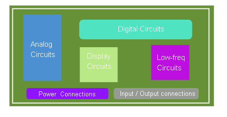
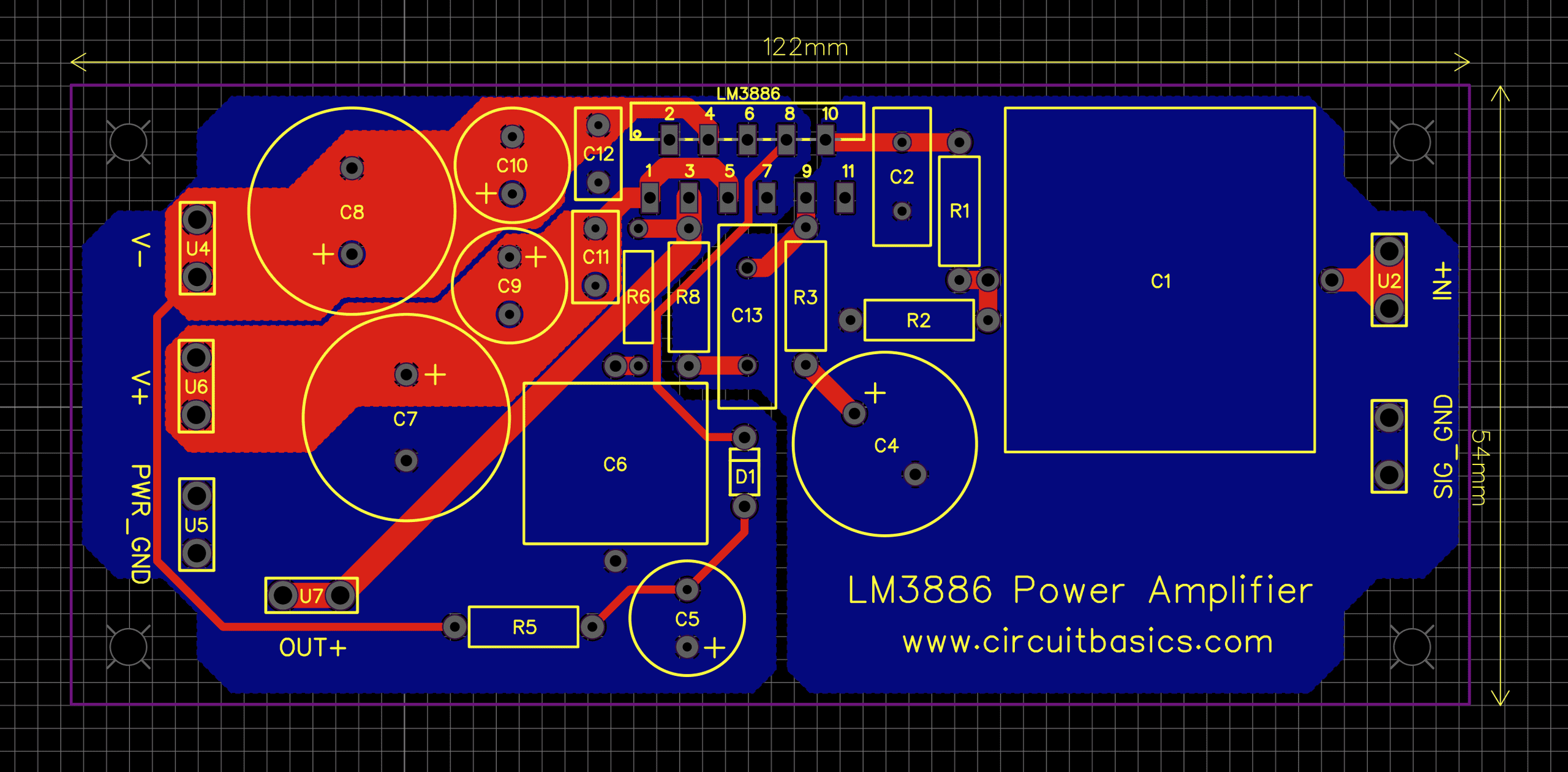
When designing a PCB, you should group the components in each sub-circuit together in different areas of the PCB. This way you can keep the track lengths between components short and have better control of the return path.
Sub-circuits that dissipate heat or generate electromagnetic fields (EMF) should be positioned away from sensitive components. For example, in an audio amplifier the noisy power supply is always placed far away from the sensitive audio input circuit.
Daisy Chain vs Star Topologies
When deciding how to arrange the different sub-circuits on your PCB, there are two common methodologies to consider – the daisy chain topology and the star topology:
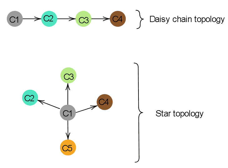
These topologies are used to describe how sub-circuits are connected to a power supply sub-circuit (C1).
In a star topology, multiple sub-circuits are directly connected to a central power supply. The advantage of the star topology is that if one sub-circuit fails, other sub-circuits will remain functional.
A daisy chain topology is when one sub-circuit is connected to the next in a chain until the circuit is returned to ground. A daisy chain topology reduces the length of traces and saves space on the PCB. But if one component fails, other components might also fail.
Design Rule Checks
Consider running a design rule check (DRC) if you want to verify whether your PCB meets the specifications set out by a set of defined geometric constraints. Design rule checking ensures that things like trace width and the spacing between components falls within pre-defined parameters. Most EDA/ECAD programs have the ability to run design rule checks on your PCB layout.
Component Placement and Orientation
When placing individual components like resistors, capacitors, or transistors into a PCB layout, arrange them in a way that minimizes the length of the conducting traces.
Aligning similar components in the same direction is also a good practice. This will give the PCB a more efficient and logical design.
For ease of access, it is usually a good practice to place any power supply connections or other input/output connections near the PCB edge.
Heat Management
Some components generate heat when an electric current flows through them. Potential heat sources may include voltage regulators, op-amps, transistors, and even copper traces and vias. You might need to employ heatsinking to remove excess heat from these devices.
If your PCB is already assembled, you can use a thermal imager to measure the heat signature of the PCB while it is operating. This can help you to identify components or sections that are emitting excessive heat.
If heat is an issue, consider replacing linear voltage regulators with switching voltage regulators. You can also use heat sinks or cooling fans. However, this could make the overall package larger and heavier.
Heat can also be dissipated from a component by using thicker copper traces. For dissipating heat way from SMD components, thermal via arrays are commonly used.
Ground Layers and Power Planes
A ground layer is a layer of copper (usually covering the entire bottom of a PCB) that is connected to the circuit’s ground terminal. PCB designers use ground layers because they can reduce or even eliminate the number and length of ground traces on the PCB.

Similar to a ground layer, some PCBs use power planes. A power plane is a large layer of copper that is connected to the circuit’s Vcc terminal. Power planes are usually added to the top of a single layer PCB or to the middle of a two layer PCB.
Using both a ground plane and a power plane can simplify the PCB design, and can reduce electromagnetic interference due to the need for less PCB traces.
Conductive Traces
The purpose of a PCB is to hold components in place and electrically connect them. The electric connections are made using conductive traces. A conductive trace is a line of copper metal on the PCB that electrically connects components.
Once you have decided where to position the different sub-circuits and how to place each component, it’s time to draw the traces that will electrically connect everything. This is a process called routing traces, and there are a variety of EDA/ECAD programs with software that makes it pretty easy.
You should also calculate how much current will flow in your circuit. This will help you determine what trace width to use so that current can flow without shorting out a trace. Use this trace width calculator to find the ideal trace width for a particular current.
How to Route Traces to Minimize EMF Noise/Interference
Recall that a moving charge produces a magnetic field, and a changing magnetic field can produce an electric field. On a PCB, electric currents of different magnitudes are flowing in different directions through all of the conducting traces. If a PBC is poorly designed, this may give rise to the creation and transmission of electromagnetic energy. This unwanted electromagnetic energy is called electromagnetic interference and this can be harmful to sensitive circuits.
As a PCB designer, there are various steps that you can use to minimize EMF noise/interference. The best way is to design your conducting traces in a way that minimizes EMF. Poorly routed traces can act as an antenna to EMF. To avoid EMF interference in your traces:
- Keep traces as short as possible
- Avoid creating loops with traces
- Avoid 90° angles in trace bends (use 45° angles instead)
- Keep high speed signals separate from low speed signals
- Keep return paths short
- Route differential (+/-) traces as close to each other as possible
Single-Layer PCBs
One of the first choices to make in PCB design is the number of layers to use. There are a lot of factors that might influence this decision. For example, the complexity of your circuit, manufacturing costs, pin density, signal layers, operating frequency, and PCB turnaround time, among others.
For most hobby projects, single or double layer PCBs are the easiest to design. Shown below is a cross section through a single layer PCB:
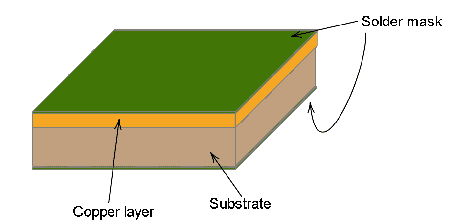
A single layer PCB has just one copper layer on the top of the PCB. This copper layer will be etched with your PCB layout files, leaving only the copper traces on the PCB. Single-layer PCBs are cost-effective, easy to understand, and convenient for manufacturing.
Double and Triple Layer PCBs
As design complexity increases, the efficiency of single-layer PCBs decrease. Highly complex PCB designs call for double-layer, triple-layer, or multi-layer PCBs.
Double-layer PCBs have two copper layers, one on top and one on the bottom:
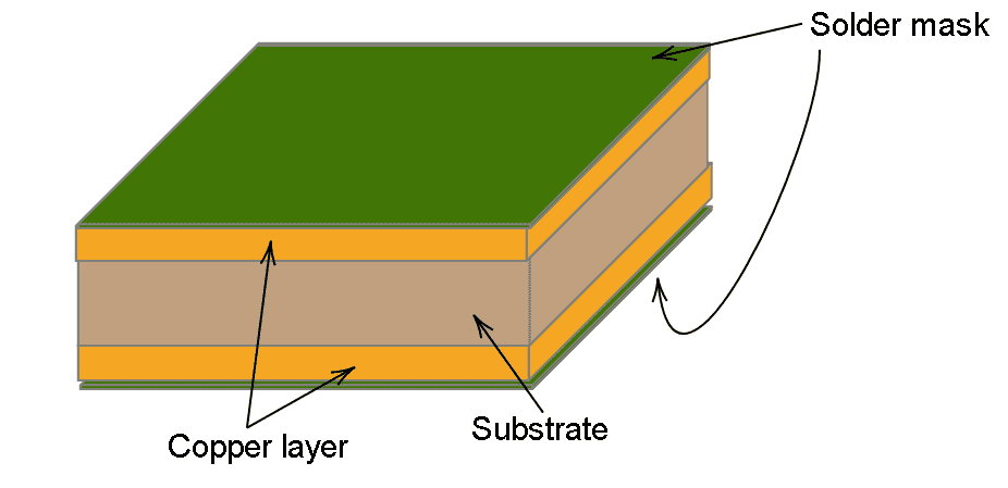
Three-layer PCBs have a copper layer sandwiched between the top and bottom layers:
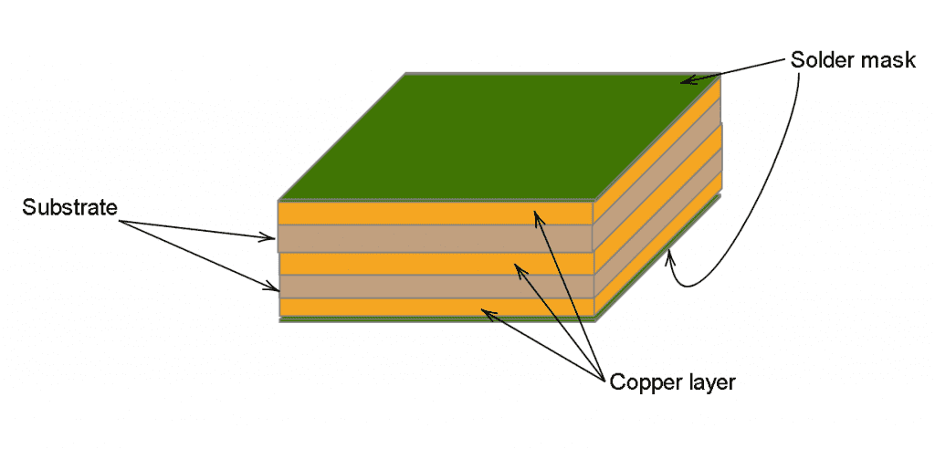
Multi-layer PCBs pack even more copper layers inside the PCB. Very complex PCBs have up to 100 layers!
Connecting the Layers
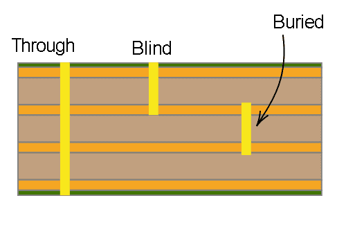
When designing a multi-layer PCB, you may need to create links between the various layers of your PCB. You can use a via to achieve that.
In Latin, via means a path or way. In the context of PCBs, vias create an electrical connection between layers in the PCB. Basically, a via is a conductive hole that has copper pads on each layer.
The three main types of vias are through-hole, blind, and buried:
Component Footprints
Before you can add a component to a PCB layout, you need to have the component’s footprint:
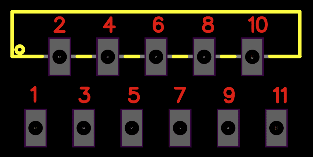
This is the component footprint for the LM3886 audio amplifier IC. The footprint defines the precise dimensions for things like component length and width, number of pins, pin layout, and diameter of through holes.
Footprints for common components are included with most EDA/ECADS. But you might need to create your own footprint for some unusual components. Most EDA/ECADs have modules that can do this easily using dimensions from the device’s datasheet.
You can also find the footprint’s for many components online, so check there first before creating your own.
The Silkscreen Layer
The silkscreen layer is used for printing text and other graphics on the PCB. This is where you will put component outlines, pin numbers, part numbers, component references (R1, C1, etc.), and any other information or logos you want to be printed on the PCB.
Gerber Files
Gerber files contain all of the information about your PCB design that is needed to manufacture it. Gerber files are the most common format for sending designs to a PCB manufacturer. Almost all EDA/ECAD programs for PCB design are able to output a set of Gerber files that you can send.
Manufacturing the PCB
Once you’ve arranged your sub-circuits, placed all of the components, and routed your traces, the next step is to send your PCB design for manufacturing.
There are many PCB manufacturers in China that offer high-quality PCB manufacturing and quick turnaround times. Most companies also offer low minimum order quantities so you can order as few as 5-10 PCBs at a time for very low prices. Search online for PCB manufacturing and you’re sure to find one that suits your needs.
Hope this article has given you some good tips and ideas on how to design your next PCB layout! Leave a comment below if you have any questions.




Good concise summery of PCB design. There is of course a lot more to it “under the bonnet” than what is described in this article, Symbols and footprints need creating and pairing. Padstacks need generating for aperture, drill and mill tables. All of which has kept me employed for over 40 years as a PCB designer.
There are lots of free utilities out there to help the design process. I can recommend using a Gerber viewer for checking your layouts before getting boards made. Just like printing out a document and spotting mistakes that you didn’t see on the screen, it can save you time and expense getting boards re-made.
As a shameless plug (I am an unpaid Beta tester) I can recommend zofzpcb (https://www.zofzpcb.com/) as a free viewer for pcb’s and it creates a 3D model of the board which looks cool when you roll it around.